 Português
  Inglês
  Espanhol
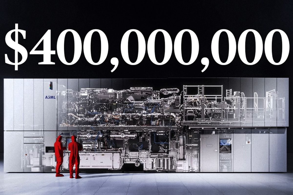


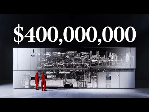
Most Complex Machine Call: ASML’s EUV Lithography Creates Extreme Light by Exploding 50,000 Tiny Droplets of Tin Per Second in Vacuum and Hydrogen, Aligning Layers with an Error of Five Atoms. With Nearly Perfect Mirrors, 20,000-Watt Lasers, and Costs in Hundreds of Millions, It Keeps Chips Evolving.
The most complex machine in the world is neither a rocket, nor a reactor, nor a supercomputer. It sits at the invisible heart of semiconductor manufacturing, where each layer of a chip needs to be created with absurd precision for billions of transistors to indeed become the ones and zeros that drive technology.
The reason is simple and brutal: the smaller the transistor, the shorter the signal path, the faster the chip processes, and the more transistors can fit in the same area. For decades, this shrinkage sustained Moore’s Law, until around 2015, when the industry began to hit a physical limit that seemed insurmountable.
Why Smaller Transistors Require an Impossible Machine
A microchip is a nanoscopic “city,” with layers and layers of structures connected by wires. At the core of it all are the transistors, in numbers that reach billions per chip.
-
A bright yellow mushroom imported from Asia escaped from a cultivation farm in the United States in 2010 and is now aggressively spreading across 25 states, destroying entire communities of native fungi in American forests.

-
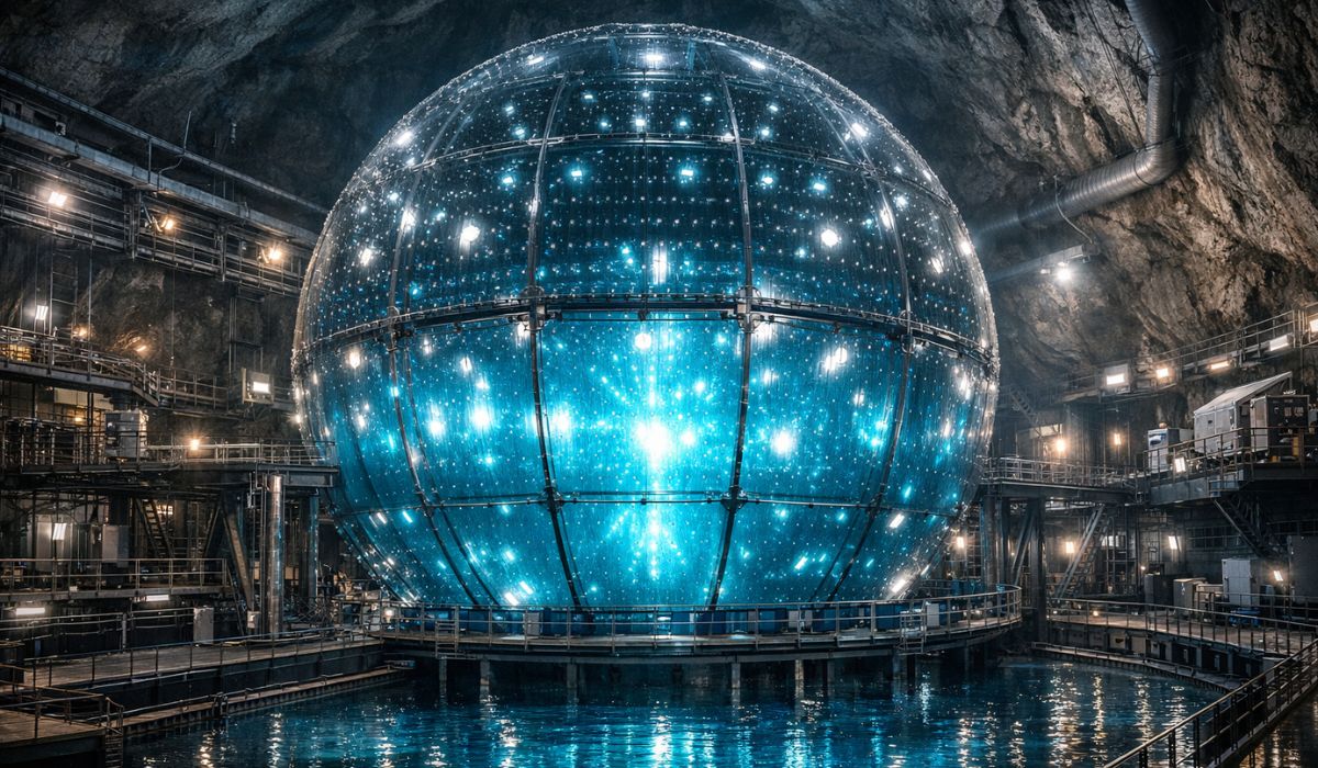
Buried under China, a colossal machine weighing 20,000 tons began operating as the largest neutrino detector on the planet and, in just 59 days, surpassed results that science took half a century to achieve.
-
Iran enters the center of a climate alert after the war emitted 5.6 million tons of CO2 in two weeks, surpassing the annual pollution of entire countries.

-
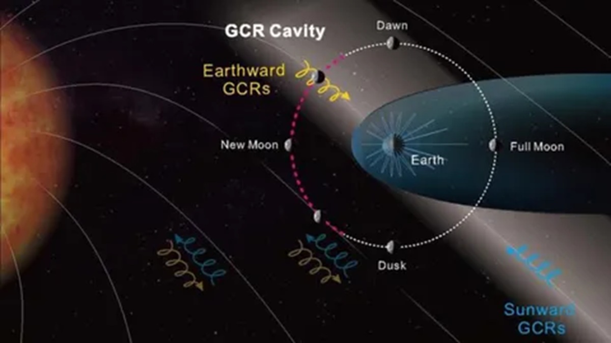
Lunar exploration may change after a Chinese probe finds a “cavity” of radiation that reduces the impact on astronauts by up to 20% at certain times on the Moon.
Manufacturing is not a single step; it’s a repeated cycle: coating with photosensitive material, exposing a pattern, etching the silicon, and depositing metal, layer after layer.
Depending on the chip, this cycle can repeat 10 to 100 layers. The layer of transistors is the most difficult, requiring hundreds of steps that need to function perfectly.
And there comes a point where everything depends on a single bottleneck: the moment the light passes through the mask and prints the design onto the wafer. That’s where the most complex machine becomes the difference between evolution and stagnation.
The Bottleneck of Photolithography and the Wall That UV Raised
Printing increasingly smaller patterns seems intuitive, but physics interferes. When the openings in the mask get close to the wavelength of light, diffraction and interference occur: the waves spread, overlap, cancel, or reinforce each other, and the design loses fidelity.
The industry pushed this limit for years with deep ultraviolet light of 193 nanometers, which sustained the most advanced chips until around 2015.
However, when the patterns become too small, simply “fine-tuning” alignment or optics is not enough: the wavelength begins to dictate the game.
The solution needed to be radical: use a much shorter wavelength and, thus, print smaller details.
This turnaround is known as EUV lithography, extreme ultraviolet. And this is where the story goes beyond “micro” and turns into engineering at the edge of what humanity can control.
EUV in Practice: Lasers, Tin in Plasma, and Mini Explosions in Series
EUV requires an environment where light is not swallowed by air, so the process occurs in vacuum. More than that: EUV light needs to be produced because it doesn’t “appear” naturally like a common lamp.
In practice, the most complex machine creates a kind of “artificial sun” on an industrial scale.
The center of the spectacle is a tiny droplet of molten tin, shot at about 250 kilometers per hour.
It is hit by sequential laser pulses, extremely precisely, to turn into plasma and emit EUV.
In one of the described arrangements, the droplet receives three impacts in 20 microseconds, heating above 220,000 Kelvin, about 40 times the temperature of the sun’s surface.
And this does not happen once: it happens 50,000 times per second.
The detail that changes everything is that tin has a peak emission around 13.5 nanometers, very close to the range used in EUV, which increases efficiency compared to alternatives like xenon.
However, tin creates a problem as big as the solution: debris and neutral atoms can contaminate the mirrors and reabsorb the EUV light itself.
To prevent particles from destroying optical components, the chamber uses low-pressure hydrogen to slow down and “clean” residues.
This hydrogen needs to circulate at extremely high speeds, and there is an explicit reference to flow reaching about 360 kilometers per hour.
The image is almost inevitable: inside the machine, “mini supernovae” happen repeatedly, and engineering needs to master thermal shock, cleaning, and stability, all at the same time.
The Smoothest Mirrors and the Alignment of Five Atoms
If EUV does not pass through common lenses and air absorbs it, the optics need to be made with special mirrors. However, reflecting EUV is not the same as reflecting visible light.
A set of multilayer mirrors is necessary, and the surface finishing needs to be so extreme that the comparison becomes almost surreal.
There is a direct description: if a mirror were enlarged to the size of the Earth, the largest protrusion would be about the thickness of a playing card.
In another comparison, mirrors from one generation would have, at the size of Germany, irregularities on the order of a millimeter.
This level of smoothness is essential because, at such small wavelengths, any roughness scatters light randomly.
And the requirement doesn’t end with reflection: the machine must overlay one chip layer over another with a maximum error of approximately one nanometer, equivalent to five silicon atoms.
Moreover, the wafer does not stay still. To achieve productivity, the system moves the stage with accelerations above 20 Gs, more than five times the typical acceleration mentioned for a Formula 1 car.
Extreme speed and precision coexist, something that seems contradictory, but is exactly what the machine delivers.
ASML, the Turning Point, and the Cost of Keeping Moore’s Law Alive
For decades, many people believed building this class of equipment was impossible.
The leap from prototype to industrial production required increasing power, boosting productivity, and making the system reliable for long periods.
A noted milestone is when development reaches 100 watts, and then aims for higher levels, such as 200 watts, because the industry demanded output compatible with a real factory.
A decisive funding mechanism also emerges: customers who depended on the technology invested heavily to keep the project going.
There are cited figures of US$ 4.1 billion in investment from Intel, and another US$ 1.3 billion combined from Samsung and TSMC to support research and development when the product was still promises and prototypes.
When commercial machines began to hit the market, orders started to pile up, and the most advanced chips became dependent on this leap.
From then on, the most complex machine ceased to be just an engineering feat and became a central piece of the global supply chain.
High NA, Clean Rooms, and the Logistics of a Colossus That Manufactures the Minuscule
Evolution continues within the product line itself. There is reference to machines with numerical aperture of 0.33 and a High NA generation with 0.55, with a larger optical system to print smaller details.
It also appears that lines in the 13 nanometer range were associated with a set, and that the most advanced generation achieves even finer results.
The assembly environment is as rigorous as the optics. In a clean room associated with construction, the stated restriction is a maximum of 10 particles per cubic meter, with about 0.1 micron.
The comparison with surgical centers is direct: operating rooms allow up to 10,000 particles per cubic meter of the same size, which showcases the level of control required.
And logistics is an industry within an industry. The machine involves a colossal supply chain, with cited figures of 5,000 suppliers, 100,000 parts, 3,000 cables, 40,000 screws, and about two kilometers of hoses.
For transport, there is a reference to a High NA machine sent in 250 containers, distributed across 25 trucks and seven Boeing 747s. It’s the ultimate paradox: to manufacture the smallest, you need to build the largest.
What This Machine Says About the Future of Chips
The story of the most complex machine is not just about an expensive piece of equipment. It’s about how the industry crossed a point where “improving a little” was not enough.
It was necessary to create a system that produces its own extreme light, keeps nearly perfect mirrors clean, moves wafers with brutal acceleration, and still delivers overlay at the atomic scale.
This set of requirements explains why a single company became central at this specific stage of the supply chain.
If miniaturization continues to require similar leaps, the future of advanced chips is likely to depend increasingly on machines that seem impossible until the day they work.
Do you think relying on a most complex machine like this is the inevitable price of advanced chips, or will the industry find another way to continue shrinking transistors without increasing the size and cost of the “colossus” around?


Podia falar que esse artigo foi inteiro baseado no último vídeo do Veritasium
Não é novidade vindo desse site. Já fizeram vários artigos em cima de vídeos do youtube
Ao mesmo tempo que o homem tem inteligência para construir uma maravilha dessa convivemos com ditadores sanguinários e até petistas!
São dois extremos absurdamente extremos da capacidade humana!
E com entusiastas da extema-direita amantes de golpes…
O cérebro do Zé deve ser como o ambiente que a máquina precisa pra trabalhar, um vácuo.. hahaha
Até onde eu lembro o **** que é amante da ****! Lambedor das bolas do ustra..
****-naro e dita-dura censurado.. Estranho.
Petistas são pessoas normais, bolsonaristas são a escória e o extrume da ignorância. Só existe UM extremo.