 Portuguese
  English
  Spanish
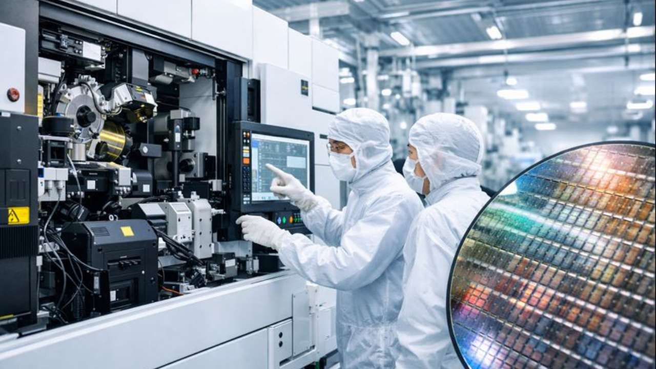


China Develops EUV Lithography to Produce Advanced Semiconductors and Reduce External Dependence in the Global Chip Industry.
In recent years, China has intensified an ambitious effort to dominate EUV lithography, a critical technology for the production of advanced semiconductors, as part of a national policy for technological autonomy.
This movement involves the government, universities, and major technology companies, primarily occurring in industrial centers like Shenzhen, advancing through coordinated research and robust public investments, and seeking to mitigate the impacts of sanctions imposed by the United States since 2018.
The central goal is to reposition the country in the chip industry and alter the balance of global technological geopolitics.
-
The heatwave in Brazil that hit in March is set to end as a cold front arrives between Good Friday and Easter Sunday, causing a temperature drop of up to 6 degrees and rain in the Central-South region, according to the Easter weather forecast.

-
The U.S. Army has introduced its first new lethal grenade since the Vietnam War: the M111 kills using pressure shock waves that bounce off walls and can explode the enemy’s lungs without producing a single shard.

-
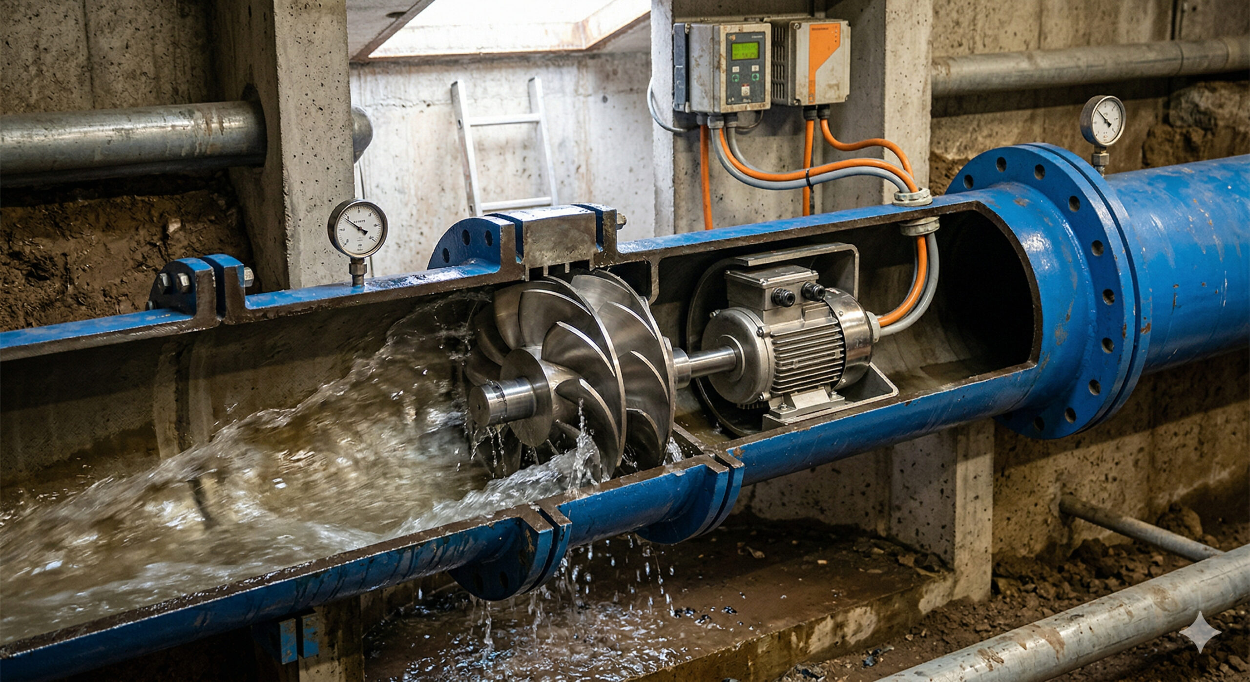
Engineers are replacing pressure valves with hydraulic microturbines within drinking water networks and are generating up to 1,100 MWh per year with in-pipe hydropower technology that harnesses energy previously wasted in urban pipelines.
-
Elon Musk focused on Brazil and lowered the price of Starlink, his internet service, but the question remains: is it worth it? An expert provides a detailed analysis of the internet that promises to connect any part of Brazil.

This strategy gained momentum after restrictions on Chinese access to sensitive equipment, particularly in the semiconductor sector.
Since then, Beijing has come to view EUV lithography as a strategic asset, essential for sustaining economic growth, national security, and long-term technological competitiveness.
What Is EUV Lithography and Why Is It Strategic
EUV lithography—short for extreme ultraviolet—is a technique used to engrave extremely small circuits onto silicon wafers.
It operates with very short wavelengths of light, allowing for chip manufacturing below 7 nanometers, the threshold for the world’s most advanced processors.
This level of miniaturization significantly increases transistor density, improves energy efficiency, and enhances computational performance.
Therefore, EUV lithography is considered indispensable for modern applications, such as artificial intelligence, high-performance computing, 5G networks, and sophisticated military systems.
Currently, few companies dominate this technology, with the Dutch company ASML being the nearly exclusive supplier of the EUV machines used globally.
Chinese Prototype Signals Reduction of External Dependence
The EUV lithography machine developed in China, still in the prototype phase, represents a significant step toward technological autonomy.
The equipment, created in Shenzhen, indicates the possibility of reducing, at least partially, dependence on foreign suppliers in the most sensitive stage of chip manufacturing.
Although the prototype is still far from large-scale commercial production, analysts believe that this technical advancement already alters market expectations.
In practice, it is a clear signal that China seeks control over the most critical links in the chip industry.
How the “Chinese Manhattan Project” Came to Be
The effort became informally known as the “Chinese Manhattan Project,” referencing the U.S. program that developed the atomic bomb in the 1940s.
This analogy highlights the project’s scale, the high degree of confidentiality, and the strategic nature of the initiative.
The program brought together thousands of engineers linked to Huawei, as well as universities and state institutes, all under centralized coordination and strong public funding.
According to reports, the development combined reverse engineering of imported components with the recruitment of former experts from foreign companies.
The technical objective is to enable, between 2028 and 2030, a stable production line for advanced semiconductors, aligned with national goals for partial self-sufficiency.
Main Technical Axes of Chinese EUV Lithography
To make EUV lithography viable on an industrial scale, China structured multiple parallel research axes.
Each front seeks to overcome bottlenecks historically dominated by a few global suppliers concentrated in Europe, Japan, and the United States.
These challenges include stable light sources and ultra-sensitive optical systems, as well as chemical materials, photomasks, and continuous maintenance processes.
Overcoming these barriers is essential to ensure reliable operation, with high yield and uninterrupted functioning.
Impacts on the Global Chip Industry
If successful, Chinese EUV lithography could challenge the dominance of central companies in the global supply chain, such as ASML itself and Taiwanese manufacturer TSMC.
The gradual entry of China is likely to redistribute productive capacities and open new supply routes.
On the other hand, experts warn that the distance between a functional prototype and the competition for global contracts is still significant.
Scaling the technology requires reliability 24 hours a day, integration with mature industrial processes, and autonomy even without unrestricted access to foreign suppliers.
Reflections for AI, Defense, and Technological Geopolitics
Thus, the advancement of EUV lithography in China has direct impacts on artificial intelligence, more efficient data centers, and command and control military systems.
By reducing external dependence, China expands its maneuvering room in national security and industrial policy.
In the international scenario, the prototype rekindles debates about export controls, intellectual property, and the relocation of factories.
Thus, the trend is toward greater technological fragmentation, with regional blocs seeking technological autonomy and reassessing risks in the global chain of advanced semiconductors.

Obrigado
China llega en un momento innecesarios de minituarización , ya que los desarrolladores se enfocan en Nueva integración y en sustituir al silicio. Aunque les servirá de experiencia