





Copper ink developed by researchers creates conductive surfaces, withstands harsh environments, and can reduce the cost of electronics manufacturing.
A layer of copper produced by printing remained preserved after spending six months submerged in seawater. The result was achieved with a reactive copper ink developed by Jun Zhang and researchers from different institutions.
The technique allows for the creation of conductive designs directly on various materials, without relying on traditional metal processing methods. The coating also showed resistance to conditions that typically promote oxidation, corrosion, and deterioration.
The work could have a significant impact on the electronics industry, which uses copper to conduct electricity in circuits, batteries, solar panels, data centers, and equipment related to artificial intelligence.
-
A printer larger than many rooms works for 72 hours in the United States and delivers an entire boat measuring 7.62 meters, weighing 2.3 tons, with a hull made of plastic and wood fibers.

-
Used cooking oil that would clog sewage networks, contaminate up to 25,000 liters of water per liter discarded, and become invisible waste is now being collected and pre-treated as raw material for biodiesel, green diesel, and sustainable aviation fuel, and in the State of São Paulo alone, there is an annual potential of 220.2 million liters of this waste.

-
Neither a planet, nor a moon, much less a common system: a discovery published in Nature reveals a mysterious celestial body with almost the mass of Jupiter orbiting a brown dwarf 71 light-years from Earth, challenging the rules of modern astronomy, questioning the traditional classifications of celestial bodies, and reinforcing that the Solar System may be just an exception amid the enormous diversity of planetary systems existing in the Universe.
-
While trying to park the car under an olive tree on his own land in Crete, Greece, a farmer saw the ground give way under the car and open a hole that was a sealed Minoan tomb of 3,400 years, with two skeletons and painted vases.


What did the researchers achieve?
The team started with a blue-colored liquid solution. After application and heating, the material forms a surface composed of copper with low electrical resistance. The process needs to occur within a temperature range of 100 °C to 150 °C.
Despite this requirement, the thermal level is lower than that needed in previous attempts to produce similar coatings. The copper ink also allows the bonding of metallic particles during this stage. At the same time, it creates a surface protection, which helps prevent the rapid degradation of the material.

The operation depends on binders produced from catechol. These substances participate in the transformation of the compounds present in the ink until the formation of metallic copper. The binders also favor the fusion between the particles at relatively low temperatures. After this union, the composition itself helps protect the layer against reactions with the environment.
The result is a flexible, conductive, and more stable coating. This combination was difficult to achieve because very thin layers of copper tend to be especially exposed to contact with corrosive substances.
Material faced acid, sulfide, and heat
The researchers subjected the samples to different conditions to observe how long the copper would remain functional. The tests involved corrosive substances and prolonged exposure to high temperatures.
The produced layer resisted for:
- more than a thousand hours in an acidic environment;
- more than 200 hours in contact with sulfide;
- more than 240 hours at a temperature of 140 °C;
- six months completely submerged in seawater.
The stay in the marine environment was one of the most severe tests. Even after this period, the printed copper remained intact, according to the results presented by the team.
Copper ink was used to print circuits
To demonstrate that the method did not work only on small laboratory samples, the researchers produced structures with different shapes and purposes. Among them were tracks responsible for the passage of electric current.
The technique was applied in:
- solar cells;
- printed circuit boards;
- a reduced replica of the Testudo statue, mascot of the University of Maryland;
- small-scale models of the Eiffel Tower.
The demonstrations also showed that the application can follow more complex designs. This broadens the possibility of using copper ink in pieces with varied shapes.
Technology could change electronics production
Within an electronic board, the metallic tracks make the connection between components and transport the current. Copper is widely used in this function due to its conduction capacity. According to Shenqiang Ren, a professor at the University of Maryland, the printed material could play the role of wiring in a new generation of equipment.
The expectation is to manufacture these devices at a lower cost, faster, and with reduced waste. The possibility of depositing the metal only in the necessary areas can also simplify production steps. In conventional processes, part of the material needs to be removed after application.

Method can replace traditional treatments
The industry uses procedures such as electroplating and chemical etching to create copper coatings and circuits. These techniques may require multiple steps, specific equipment, and the use of chemicals. The new approach seeks to form the metallic design directly on the surface.
With this, researchers hope to reduce manufacturing time and the amount of waste generated. The method can also reduce expenses related to processing. However, its commercial adoption will depend on the ability to scale up production while maintaining the same quality achieved in experiments.
Copper can take a place today reserved for silver
Some conductive inks use more expensive metals to ensure stability and efficient current flow. Silver is among the materials used in these applications. The team believes that copper ink could offer a more economical alternative.
The goal is to take advantage of a metal widely used in the industry without facing the oxidation problems that limited its application in printed layers.
Liangbing Hu, a member of the study, stated that the technology has the potential to expand the use of copper in electronic, energy, and environmental applications currently served by higher-cost materials.
Use goes beyond circuit boards
Electrical conduction is present in different technologies of everyday life. Communication systems, photovoltaic panels, and batteries depend on metallic connections to function. Copper is also essential in artificial intelligence infrastructures and data processing centers.
In these environments, large amounts of the metal are used in electricity distribution and in connecting components. A simpler printing technique could serve small parts and surfaces with specific geometries.
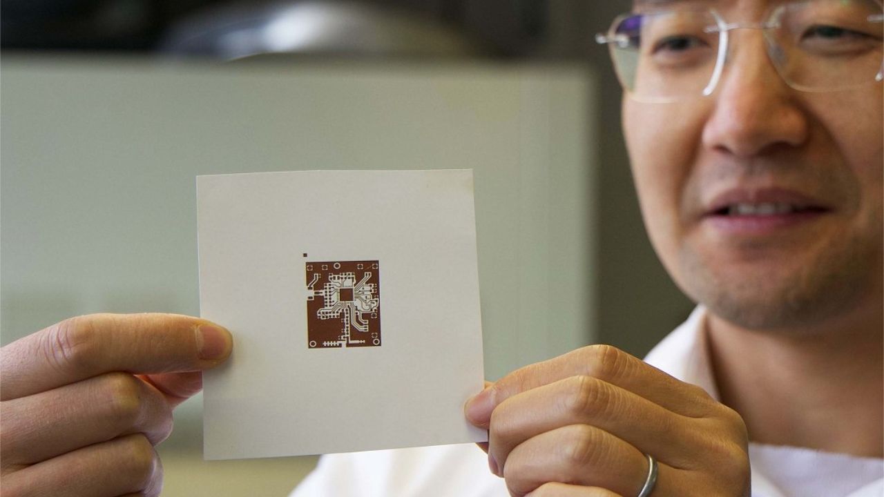
The flexibility of the material also opens up possibilities for devices that do not use completely rigid structures. The research addressed two important obstacles: allowing the printing of copper in environmental conditions and reducing the metal’s exposure to corrosion after application. Nevertheless, the process does not occur without heating.
The surface needs to withstand temperatures of at least 100 °C. This may limit use in heat-sensitive materials or require adaptations in manufacturing. On the other hand, the maximum temperature of 150 °C is considered low compared to previous experimental methods. This difference may facilitate the integration of the technique into some production lines.
Copper ink can reduce wasted materials
Direct printing allows the conductor to be positioned only in the design defined by the project. In this way, the manufacturer would not need to coat a large area to later remove unnecessary parts.
This feature can reduce the consumption of metal and substances used to remove the excess. It can also shorten the number of steps between surface preparation and obtaining the final circuit.
The copper ink will still need to advance beyond laboratory tests before replacing large-scale industrial processes. The results, however, show that the metal can be printed, remain conductive, and withstand long periods even in harsh conditions.
The research was published in Science, see here


