 Portuguese
  English
  Spanish
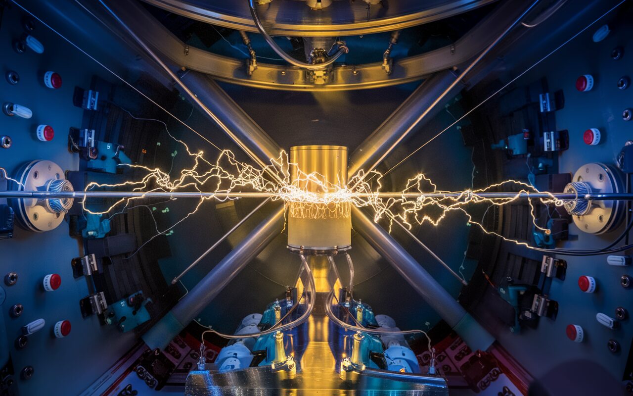
New Ultra-Thin Niobium Wire Surpasses Copper In Electrical Conductivity By Up To Six Times And May Revolutionize Sectors Like Electronics, Energy, And Superconductors In The Near Future.
An innovative discovery promises to transform the way we handle electrical conduction in electronic devices. Scientists from Stanford University have developed an ultra-thin niobium wire with electrical conductivity up to six times greater than that of copper, which could directly impact the performance of chips, integrated circuits, and data centers in the near future.
The new material, based on niobium phosphide (NbP), breaks historical barriers in materials science and may usher in a new generation of electronic interconnections, where energy efficiency and miniaturization are crucial factors.
Understand Why Niobium Wire Surpasses Copper In Ultra-Thin Scales
Traditionally, copper is the material of choice when it comes to electrical conductivity. With a conductivity of 5.96 × 10⁷ Siemens per meter (S/m), it easily outperforms other metals in practical applications. In contrast, conventional niobium has significantly lower conductivity, at just 6.7 × 10⁶ S/m.
-
Argentina achieves the unimaginable after more than 110 years and reintroduces the largest native herbivore of South America to the Chaco to restore a lost link in nature.

-
Returning to the Moon now costs a billion-dollar bill and reignites the competition between the USA and China for science, technology, and rare minerals on lunar soil.

-
While the world looks at oil, the war with Iran is already disrupting helium supply from Qatar, affecting car and iPhone chips, threatening AI expansion, and putting pressure on aluminum packaging at the highest value in four years.

-
Global warming will expose a treasure hidden under the ice of Antarctica and may spark an international dispute over gold and valuable minerals.

However, when it comes to materials at the atomic scale, physical properties behave differently. Instead of losing efficiency when miniaturized — as copper does — the ultra-thin niobium wire has demonstrated a dramatic increase in conductivity as its thickness is reduced to a few nanometers.
The niobium phosphide wires, with a thickness of just 1.5 nanometers, exhibited conductivity up to six times greater than that of copper at the same scale.
According to researcher Asir Khan, lead of the study, “we are breaking a fundamental bottleneck of traditional materials like copper. Our niobium phosphide conductors show that it is possible to send faster and more efficient signals through ultra-thin wires.”
The Secret Of Performance: Topological Semimetals
The phenomenon that allows the ultra-thin niobium wire to surpass copper is linked to the unique properties of so-called topological semimetals.
Niobium phosphide (NbP) is classified as a topological semimetal, meaning that while the material conducts electricity in its internal volume, its surfaces are even more conductive. Thus, as the wire thickness decreases, the highly conductive surface begins to dominate the electrical behavior of the material.
This behavior is completely different from conventional metals. In copper, for instance, as the wire thickness is reduced, electrical conductivity tends to decrease dramatically due to increased scattering of electrons at the surfaces. In niobium wire, the opposite occurs: the thinner it gets, the more efficient it becomes.
Researcher Akash Ramdas, also involved in the project, highlighted: “It was believed that to take advantage of these topological surfaces, it would be necessary to obtain high-quality monocrystalline films, which would be impractical. But now we have another class of materials — topological semimetals — that make this feasible in conventional industrial processes.”
Impacts On The Future Of Electronics And Energy Efficiency
The main impact of the new niobium wire is the potential to significantly improve the energy efficiency of electronics. With lower electrical resistances, circuits will be able to operate with reduced energy losses, decreasing the heating of components and increasing the lifespan of devices.
In applications such as data centers, which consume immense amounts of energy for processing and cooling, even small improvements in electrical efficiency can lead to million-dollar savings and drastically reduce associated carbon emissions.
The ultra-thin niobium wire could be integrated into:
- Next-Generation Integrated Circuits (Chips).
- Printed Circuit Boards For Smartphones And Computers.
- High-Speed Communication Networks.
- Edge Computing Equipment.
- Aerospace And Artificial Intelligence Applications.
The fact that niobium phosphide can be deposited at low temperatures is also crucial: it is compatible with existing production lines in the semiconductor industry, eliminating the need for massive investments in new infrastructure.
How The Discovery Was Made: Challenges And Next Steps
The study involved advanced techniques for thin-film growth, high-resolution electron microscopy characterization, and electrical transport testing under extreme conditions.
According to scientists, the next step is to integrate the ultra-thin niobium wire into functional prototypes of chips and circuit boards. The team has already begun partnerships with semiconductor manufacturers to assess the scalability of the technology.
The goal is to gradually replace copper interconnections at critical levels of miniaturization, where traditional material becomes unfeasible due to physical limitations.
Comparison: Copper Vs. Ultra-Thin Niobium Wire
| Property | Copper (Bulk) | Ultra-Thin Niobium Wire (1.5 Nm) |
|---|---|---|
| Electrical Conductivity | 5.96 × 10⁷ S/m | 6x Superior To Copper At The Same Thickness |
| Behavior In Thin Thicknesses | Degrades | Improves |
| Type Of Material | Conventional Metal | Topological Semimetal |
| Processing Temperature | High | Low (Compatible With Chip Manufacturing) |
| Potential For Nanoelectronics | Limited | Very High |
Source: Stanford University (2025)
Ultra-Thin Niobium Wire: A Quiet Revolution In Electronics
The creation of the ultra-thin niobium wire represents a watershed moment for the electronics industry. In an increasingly dependent world on fast processing and efficient energy consumption, innovations like this will be key in sustaining the growth of emerging technologies such as quantum computing, 5G/6G, artificial intelligence, and the Internet of Things.
While still in the early stages of commercial application, the new conductor based on niobium is yet another demonstration of how materials science can redefine the limits of what is possible in the world of technology.
With this, the ultra-thin niobium wire establishes itself as one of the most promising bets for the future of integrated circuits, rivaling the historical dominance of copper and opening new possibilities for an era of faster, more efficient, and more sustainable electronics.


-

Uma pessoa reagiu a isso.