


 Portuguese
 Spanish


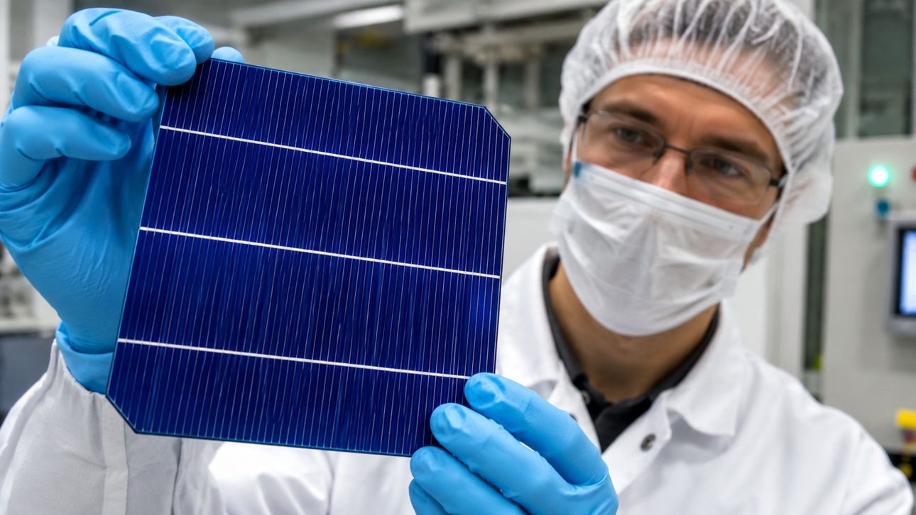

Comparisons using computational models indicate that certain nanostructures can retain the antireflective behavior associated with black silicon while exposing less surface area. The result concerns geometry and optical response, not an equivalent reduction in raw material use or proven electrical efficiency.
Microscopic structures created on the surface of silicon can reduce the amount of light reflected without requiring the same surface area found in configurations used to represent so-called black silicon. The finding comes from simulations conducted by a team that included researchers from the University of São Paulo (USP) and the University of York.
The result seeks to reconcile two characteristics that do not always go hand in hand in a solar cell: allowing more light to enter the silicon while limiting the extent of the structured surface. A very large surface area can create challenges for the behavior of electrical charges, even when the optical response is favorable.
-
Solar window tested by Brazil’s Federal University of Paraíba generated over 90 watts under high irradiance, combining power generation with heat control on a building facade

-
Mexican Miner Secures 20-Year Solar Power Deal for 269-MWp Project with Battery Storage, Supply Starting in 2029
-
Wind energy association challenges in Brazil’s Supreme Court over battery cost rule ahead of December auctions
-
Copel assembles seven pumped-storage hydropower projects totaling about 9 GW in Paraná and seeks contracts in future energy-storage auctions
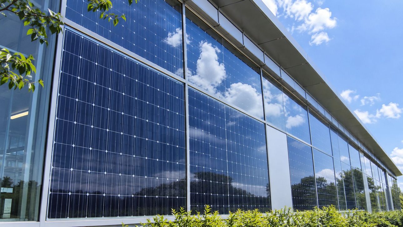
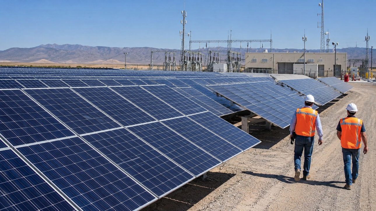


The study was published in the IEEE Journal of Photovoltaics in 2020 and used computational models to compare different geometries at dimensions close to the wavelengths of light. The study does not present a commercial panel or a complete photovoltaic device ready for mass production.
Why black silicon reflects little light
The name black silicon refers to the dark appearance the material takes on when its surface is structured to sharply reduce reflection. In a photovoltaic application, this characteristic matters because less of the incoming radiation is reflected back into the environment before entering the material.
The amount of light that reaches the inside of the silicon, however, is only part of the problem. To generate electricity, a cell also needs to generate and transport charges efficiently, a process that can be hindered by surface characteristics and recombination mechanisms.
That was the focus of the researchers’ comparison of the geometries. The simulations assessed conical structures that could have antireflective properties similar to those attributed to black silicon, but with less than half the surface area of some configurations used as benchmarks.
The term “surface area” has a specific meaning in this context. It refers to the extent of the exposed surface created by the microscopic relief of the structures, not the total amount of silicon in the device or the mass of raw material needed to produce a panel.
For that reason, the result does not support the claim that a cell built with this geometry would use half as much silicon. Nor does it demonstrate an equivalent reduction in cost, weight, or the amount of industrial material, factors that would depend on the complete design and manufacturing process.


Optical response is not the same as cell efficiency
The team investigated how different shapes could maintain low reflectance without reproducing such an extensive surface. The paper, also available in the White Rose academic repository, describes a comparison of structures at the scale of light and their calculated optical behavior.
In addition to reducing reflection, a photovoltaic structure can be designed to promote the path of light through silicon. These effects are related but not identical: allowing radiation to enter and increasing its absorption depend on how the surface and interior of the material interact with different wavelengths.
The simulations made it possible to test these geometries under comparable conditions before any manufacturing stage. This type of modeling helps identify configurations that warrant experimental investigation, especially when producing each physical variation would require micro- or nanofabrication processes.
The study indicates that certain conical arrangements can preserve desirable optical characteristics while reducing the exposed surface area compared with the black silicon model considered by the authors. The conclusion remains limited to the calculated behavior of the structures, not the electrical output of a complete solar cell.
This distinction prevents the comparison from being interpreted as a proven gain in photovoltaic efficiency. Converting light into electricity also depends on material quality, interfaces, control of electrical charge recombination, and other device characteristics that cannot be replaced by an isolated optical result.
The same limitation applies to any potential industrial application. A geometry that performs well in simulation must still be manufacturable with adequate control over its dimensions and surface properties, and must maintain its performance when integrated with the other layers and components of a solar cell.
What still needs to be demonstrated in practice
The work does not give a commercial launch date for the structure analyzed or forecast when it might replace available panels. Nor do the simulations specify how much electricity a cell built using this configuration would produce.
The study’s contribution is to identify, within the model used, a way to pursue the optical effect of black silicon without necessarily retaining such an extensive surface. This reduction could be relevant to research seeking to balance interaction with light and the electrical effects associated with structured surfaces.
The next step in evaluating this approach depends on experiments with real devices. Fabricating the nanostructures, characterizing the materials, and taking electrical measurements of complete cells would be necessary to determine whether the properties observed in the simulations persist when the geometry is produced and integrated into a photovoltaic device.