



 Portuguese
  Spanish


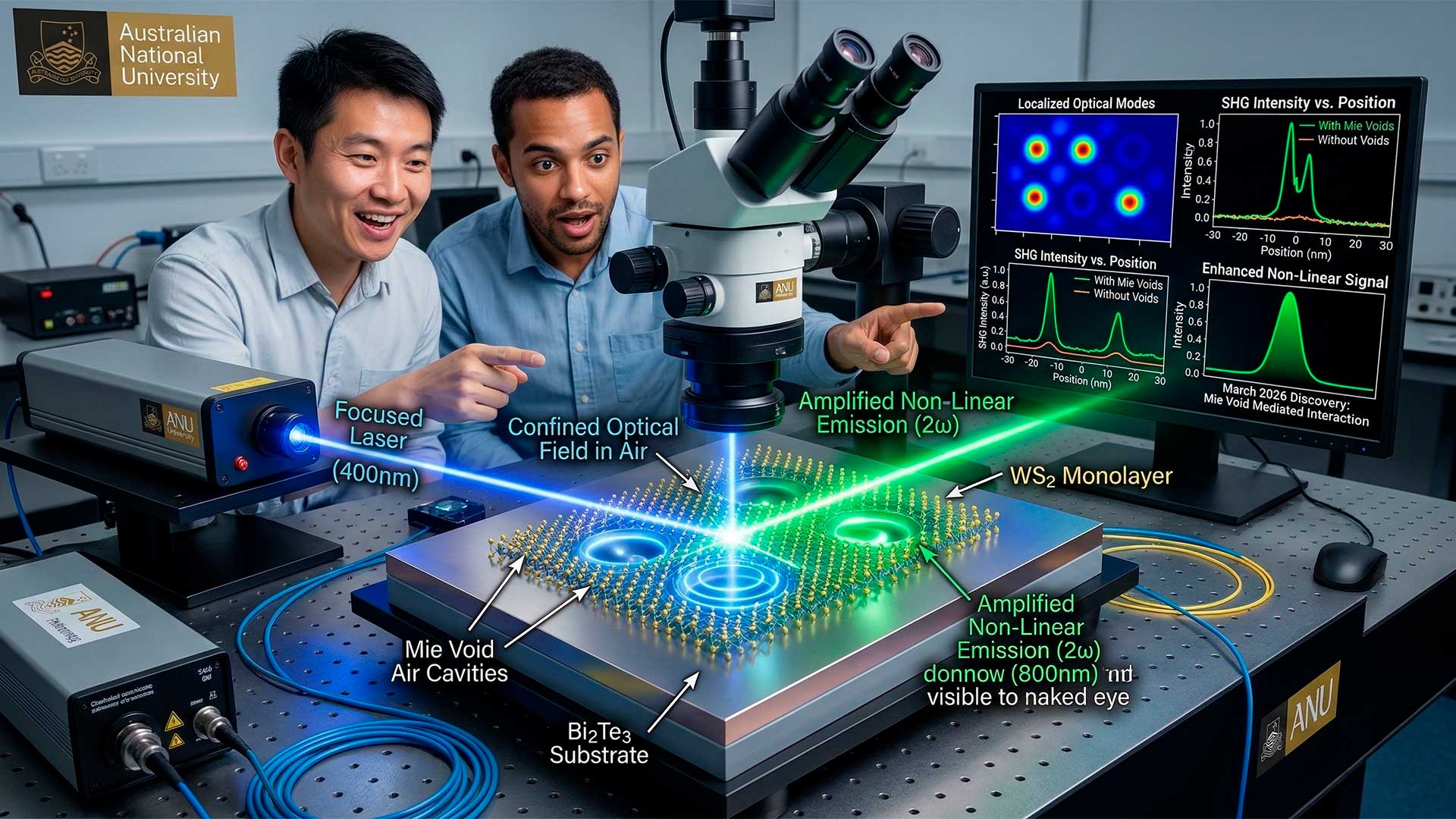


Researchers Show That Vacuum Can Work In Favor Of Photonics By Confining Light In Cavities Smaller Than The Wavelength. The Strategy Elevates Light-Matter Interaction In Van Der Waals Materials And Boosts Nonlinear Signals Without Altering Atomic Layers
In March 2026, a team led by Zhuoyuan Lu from the Australian National University demonstrated a simple yet powerful way to solve an old problem of van der Waals materials. These two-dimensional semiconductors are ultrathin, which limits the amount of light they can interact with and, consequently, weakens emissions and second harmonic generation. The solution came from where it was least expected, from the empty space between the layers.
Instead of manipulating atomic stacking, scientists decided to trap light in air, near the active surface of the material. This way, the optical field spends more time confined in the vicinity of the monolayer, intensifying nonlinear optical processes and making emission much more efficient. According to researchers at the Australian National University, the method opens new avenues for integrated photonics and surface sensing.
The approach revolves around the so-called Mie cavities, small air cavities sculpted in a high refractive index crystal. By placing a monolayer of tungsten disulfide (WS2) over these cavities, the team was able to concentrate the optical field exactly where it is most useful, in the air close to the active material.
-
Artist’s 15-Meter Lighthouse in the Mojave Desert, 160 km from the Sea, Intrigues Visitors with 19 km Range After Years of Bureaucracy

-
Bluetti AC70 Solar-Powered Station: Powers Fridge and Wi-Fi During Blackouts, Delivers 1,000W, 3,000 Charge Cycles, Priced at $900

-
Enormous Black Hole Phoenix A* Challenges Scientific Understanding with Mass of 100 Billion Suns, Surpassing Famous TON 618 in One of the Largest Known Galaxy Clusters
-
Say Goodbye to Storing Wine in a Regular Fridge: Midea’s Climate-Controlled Cellar Holds 34 Bottles, Maintains 5-18°C, and Uses Only Half a kWh Daily


The result was a measurable leap in light emission and nonlinear signals, with direct visualization of localized optical modes.
Mie Cavities In Air, The Trick That Inverts The Logic Of Resonators
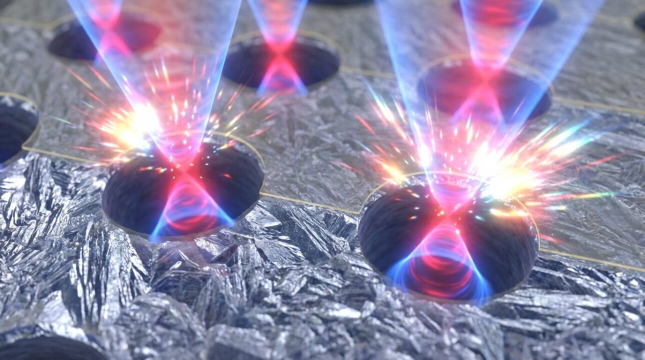
Traditionally, dieletric nanocavities confine light within solids like silicon, which works well in many scenarios. The problem is that these fields are far from the surface of the monolayer that really needs to do the work, losing efficiency in light-matter interaction. Furthermore, when the host material absorbs light, the resonances weaken and the field intensity decreases.
The Mie cavities operate in an opposite and elegant manner. Instead of holding light in the material, they keep it spinning within air cavities smaller than the wavelength, carved into a dielectric with a very high refractive index.
The strong reflection at the air-dielectric interface conserves energy in the cavity, with the optical field concentrated in the air and sticking to the active monolayer, which maximizes interaction and accelerates nonlinear phenomena.
From WS2 To Bi2Te3, How The Hybrid Platform Concentrates The Optical Field
The core of the experiment is a simple and reproducible hybrid platform. A monolayer of WS2 is positioned over nanoscale depressions carved into bismuth telluride (Bi2Te3), a material with a high refractive index that favors the formation of Mie resonances. The cavities function as air “traps” in which light remains trapped long enough to interact intensely with the WS2.
By keeping the optical field in the air but attached to the surface of the monolayer, the platform avoids absorption losses in the solid host and overcomes the distance that previously separated light from the active material. According to the team, this significantly increases light emission and frequency conversion, with a clear gain in second harmonic generation and other nonlinear signals.
Another crucial point is the ability to directly visualize the localized optical modes, something difficult in conventional architectures. This direct reading helps optimize cavity design, adjust target wavelengths, and spatially program photonic devices based on 2D semiconductors. In practice, fine control of the vacuum becomes a design variable as relevant as the choice of material.
In WS2, widely studied for quantum optics and on-chip light sources, the interaction gain solves a chronic bottleneck of ultrathin materials. By positioning the material in the right place of the field, the platform delivers what matters, more light where the material is. Bi2Te3, in turn, acts as a high-index support that sustains the Mie cavities without competing for optical energy in the volume.
This WS2 plus Bi2Te3 combination exemplifies a modular strategy that can extend to other monolayers and high-index hosts. The roadmap is clear, design the vacuum as an active element of the device, not just the solid.
Impact On Nonlinear Optics And Sensing, From Second Harmonic To Programmable Photonics
With the intensified optical field near the monolayer, processes like second harmonic gain efficiency and become detectable with lower pump power. This is vital for on-chip integrated light sources, which require low energy, compactness, and stability to operate on a large scale. The same applies to optical memories and photonic processors, areas where every decibel of gain makes a difference.
In surface-enhanced sensing, the proximity of the field to the monolayer favors the detection of small changes in index or molecular adsorption.
Small variations in the immediate environment alter the localized optical response, allowing the detection of weak signals with high sensitivity. It is a promising avenue for biosensors and chemical monitoring in nanoseconds.
The ability to spatially program the response, shaping the arrangement of the cavities and the position of the monolayers, enables reconfigurable architectures. This opens the door to programmable photonic devices, frequency conversion matrices, and nonlinear metasurfaces capable of generating beams and colors on demand. Here, engineering the vacuum becomes a fine-tuning knob for advanced functions.
What Differentiates From Dielectric Nanocavities, Limits And Next Steps
Unlike traditional resonators, which confine light in the solid mass, the Mie cavities concentrate the field in air without moving away from the active surface of the 2D. This reduces absorption losses in the host and improves the overlap between field and material, two decisive factors for the strength of nonlinear processes. According to researchers at the Australian National University, this deviation explains the observed leap in emission and frequency conversion.
Among the next steps are the precise adjustment of the cavity geometry, coupling with other monolayers of van der Waals materials, and integration into on-chip platforms. More broadly, the study reinforces a simple yet powerful thesis, modeling empty space may be as important as choosing the material, especially when scale falls to nanoengineering.
Is modeling the vacuum as revolutionary as it seems or just another trend in 2D materials photonics? Do you see real advantages over classical nanocavities, even considering manufacturing challenges and long-term stability? Leave your comment and tell us if you would bet your next prototypes on this architecture based on Mie cavities.