
 Portuguese
  Spanish
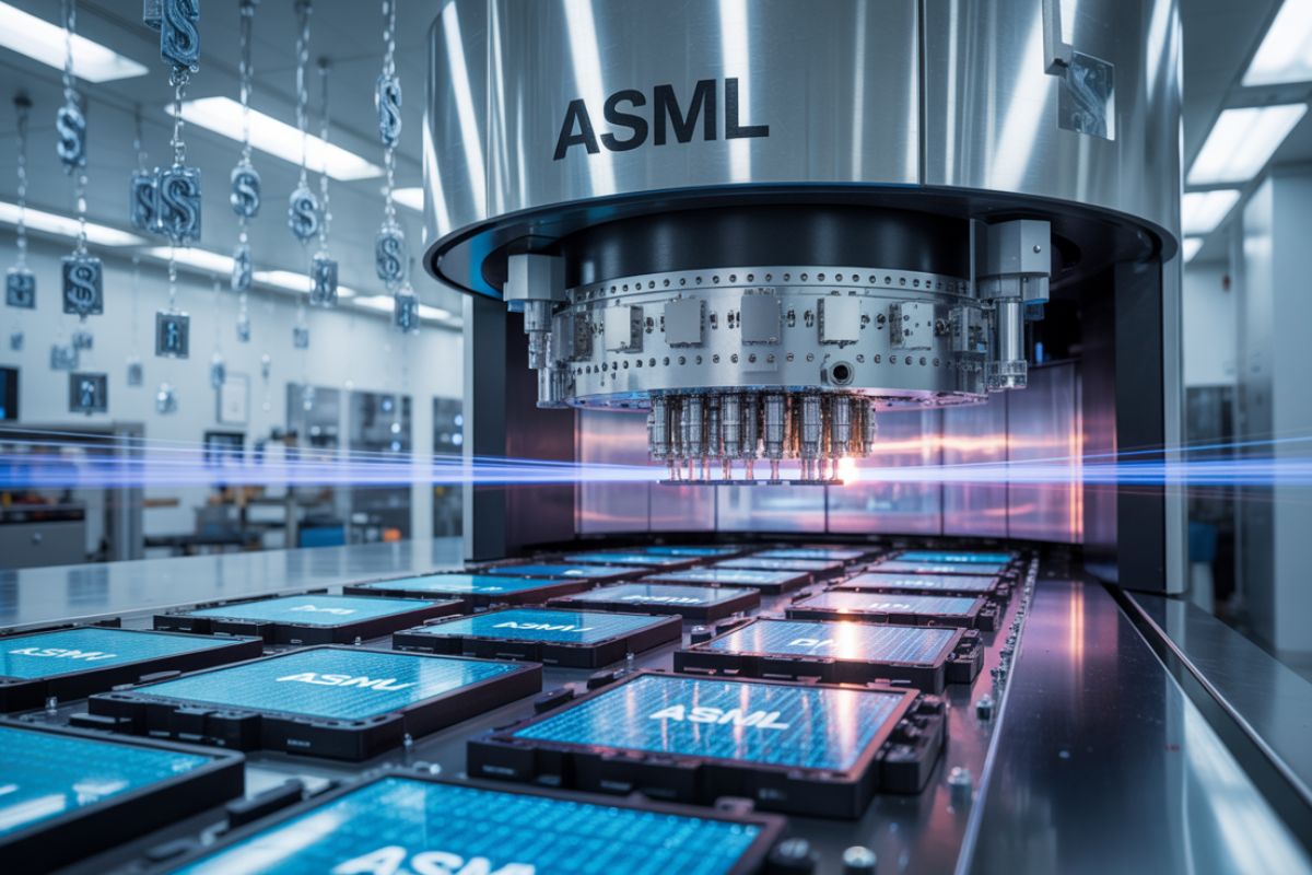
Meet ASML’s EUV High-NA Technology, The Equipment That Defines The Future Of Artificial Intelligence And Semiconductors And That Only Three Companies In The World Can Purchase.
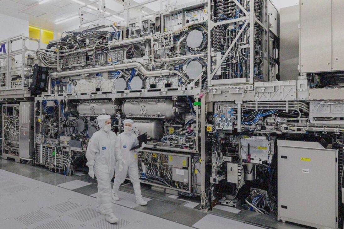
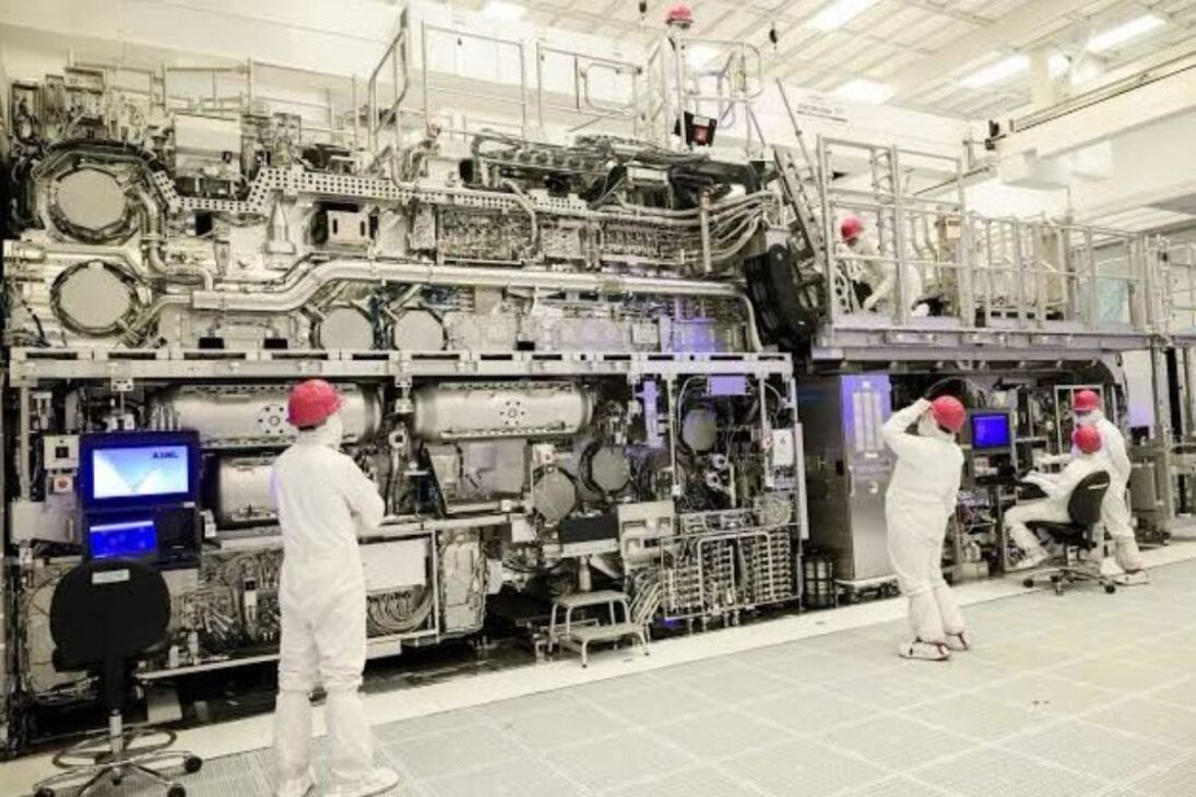
In a quiet and ultraclean laboratory in the Netherlands, locked behind reinforced doors, is the most important piece of technology on the planet. It is not a secret formula, but a machine the size of a double-decker bus that costs US$ 400 million. This equipment is the reason how a single US$ 400 million machine is dominating the chip world, and it belongs to a single company: ASML.
Giants like Intel, Samsung, and TSMC are in a fierce race to secure their units, for without them, the advancement of artificial intelligence, smartphones, and the entire digital economy simply stops. The key to all of this lies in mastering light in a way that borders on science fiction, creating circuits billions of times smaller than a grain of sand.
The Light That Cuts Through The Invisible
To understand ASML’s power, it is necessary to know its exclusive technology: extreme ultraviolet (EUV) lithography. It involves using a beam of light with a wavelength of only 13.5 nanometers — so short that it is absorbed by practically everything, including air. Therefore, the entire process must occur in a perfect vacuum.
-
Mother from Brazil’s Maranhão Creates Lactose-Free Cookie for Daughter with Cerebral Palsy, Now Producing 10 Tons Annually and Exporting to Mexico

-
Brazilian Student Turns Electric Shower Repair into Thriving Industry with 3,600 Jobs and Over $1 Billion in Revenue, Aiming to Become the “Next WEG”

-
German Ship Concludes 40-Year Maritime Career with Final Mission in Brazil, Departing Recife with Floating Labs to Study Atlantic Currents
-
Artisanal Well Transforms 4 Hectares in Brazil’s Semi-Arid Region into Productive Farmland with Drip Irrigation


The generation of this light is an engineering spectacle:
50,000 droplets of liquid tin are fired per second inside the vacuum chamber.
Each drop is precisely hit by a high-power carbon dioxide laser.
The impact generates a ball of plasma hotter than the surface of the Sun, which emits the necessary EUV light photons.
This light cannot pass through common glass lenses. Instead, it is reflected by a series of mirrors made by Zeiss, considered the flattest surfaces ever created by humanity. If Earth were as smooth as one of those mirrors, the tallest mountain would be just a few millimeters high. All this effort serves a single purpose: to “print” circuit designs on a silicon wafer, creating billions of transistors that are 10,000 times thinner than a human hair.
What Makes The New High-NA Machine So Special?
The machine that costs US$ 400 million is the next generation of EUV technology, called “High-NA” (High Numerical Aperture). The numerical aperture refers to the system’s ability to capture more light at wider angles. In practice, this allows for smaller and more complex circuit patterns to be etched in a single exposure.
This represents an industrial revolution. Rather than exposing the silicon wafer multiple times to create a single layer of a chip (a costly and error-prone process), the High-NA machine can do the work in fewer steps. The result is faster production, with fewer defects and ultimately more powerful and efficient chips.
This precision, however, comes with an immense logistical cost. Each High-NA machine consists of over 100,000 parts and 2 kilometers of cables, and its transportation requires a fleet of seven Boeing 747 cargo planes and dozens of trucks.
ASML’s Monopoly: From A Cabin To Global Control
The story of how a single US$ 400 million machine is dominating the chip world began humbly. In 1984, ASML was born in a makeshift shed in Eindhoven, the Netherlands, as a subsidiary of Philips. While the world bet on safer technologies, a small group of engineers decided to invest in the almost impossible idea of EUV lithography.
For more than 20 years, they repeatedly failed, but persistence paid off. Today, ASML is the only company in the world capable of producing EUV lithography machines. Without it, giants like Apple, Nvidia, and Intel simply couldn’t manufacture their most advanced processors. It is an absolute technological monopoly, built over decades.
Why Is China Left Out?
While Intel, TSMC, and Samsung compete for the few available High-NA machines, a crucial player is out of the game: China. Due to a political decision led by the United States, the sale of any EUV technology machine to Chinese companies has been prohibited.
The goal is clear: to prevent China from developing next-generation chips for use in advanced artificial intelligence and military applications. In response, China has been stockpiling machines from the previous generation (DUV) and investing billions to try to develop its own technology, but replicating ASML’s ecosystem, which involves hundreds of specialized suppliers, is considered by many an almost impossible task.
The Energy Dilemma And The Future Of Chips
Despite the technological advances, there is an obstacle that could hinder progress: energy consumption. The High-NA EUV machines are extremely “greedy” for electricity. ASML itself admits that consumption is a challenge.
The alert is serious: if the energy efficiency of chips does not improve drastically, training AI models and operating data centers could become unsustainable. With the demand for chips growing exponentially, the technological race has also become an energy race.
The saga of how a single US$ 400 million machine is dominating the chip world is the story of technology at its extremes. It shows how persistence in an audacious idea can lead to a global monopoly, but also exposes the complex battles and sustainability challenges that will define the future of our digital civilization.
In your opinion, is ASML’s monopoly a risk to the world or a guarantee of technological stability? Leave your comment!


