Portuguese
  Spanish
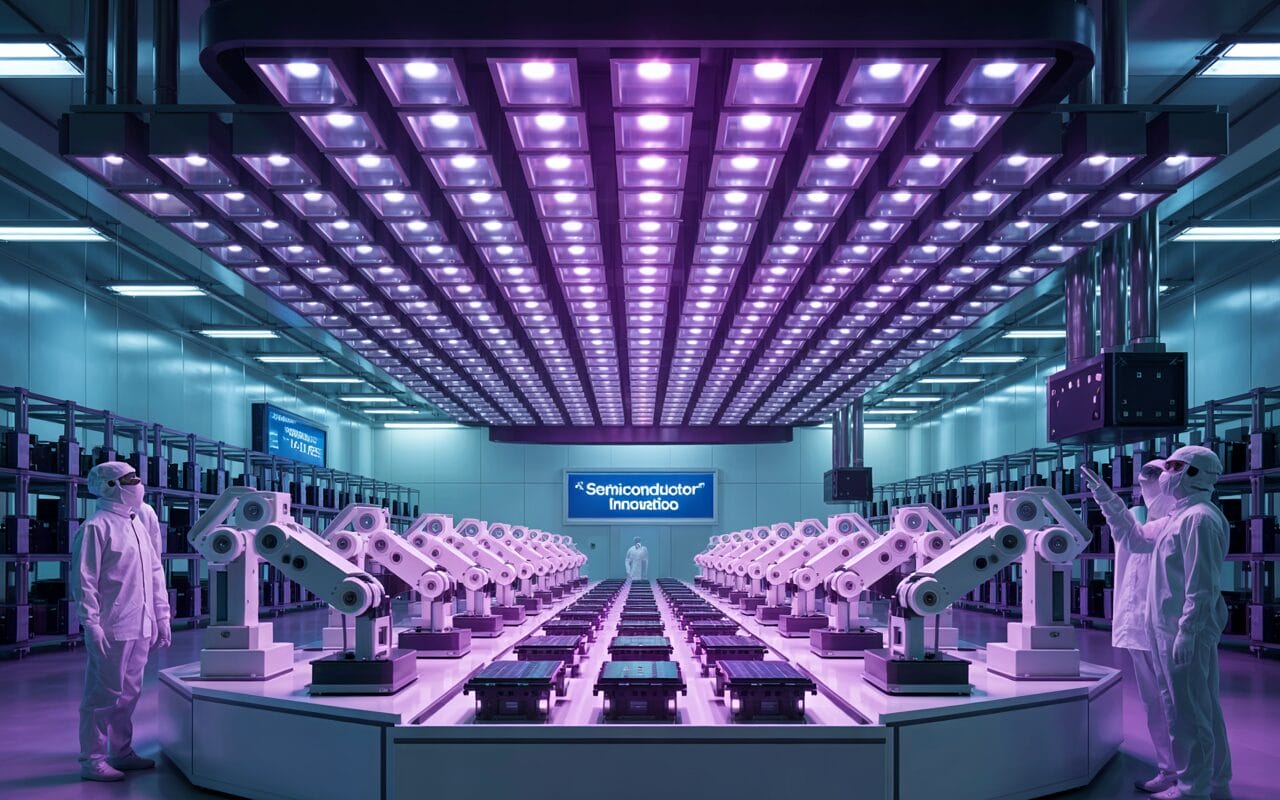
China Will Use Particle Accelerator to Produce Mega Source of Ultraviolet Light. Understand How This Strategy Could Change the Global Semiconductor Sector.
For several years, China has been working on its own Manhattan Project. Unlike the plan executed by the United States during World War II, this project is not aimed at the production of nuclear weapons, which China has owned since the mid-1960s. It is about the production of a device that is gaining competitiveness in the global semiconductor market. In this article, we will detail the semiconductor race and how the mega source of ultraviolet light will enable the production of these components.
Understand China’s Objective with the Semiconductor Project
The focus of the Asian country is to give companies the ability to produce cutting-edge integrated circuits, comparable to the most advanced ones currently produced in Taiwan, the USA, Japan, and South Korea. The sanctions imposed by the governments of the USA and the Netherlands are preventing ASML from delivering its most advanced photolithography equipment, such as extreme ultraviolet (EUV) machines, to its Chinese customers.
Without equipment, Chinese semiconductor companies, such as Semiconductor Manufacturing International Corp (SMIC), Hua Hong Semiconductor, China Resources Microelectronics, and Guangzhou ZenSemi cannot manufacture integrated circuits equivalent to those already produced by Intel, Samsung, or TSMC. Therefore, the Asian country needs to have its own mega source of ultraviolet light as soon as possible. Its economy, and especially its technical and scientific development, is at stake.
-
Seventh Grader Builds Nuclear Fusion Machine at Home, Aiming for Guinness World Record

-
Ancient Ritual Circle, Hidden for 5,000 Years, Discovered in Scotland’s Machrie Moor Using Sensors, Revealing a “Phantom Stonehenge”

-
Engineers Develop Fridge-Sized Machine to Produce 95-Octane Synthetic Fuel from Air and Water, Aiming to Sustain Combustion Engines Without Oil
-
Two-Armed Robot Uses AI to Reassemble Destroyed Pompeii Frescoes, Solving an “Impossible” Puzzle


However, the problem is that creating a machine to produce the components is very complex. In fact, ASML took more than two decades to perfect it and also received economic support from its clients such as Intel, TSMC, and Samsung, in addition to partnerships with several companies that hold cutting-edge technologies, such as the German Zeiss, which produces the optical elements of the lithography machines, and the American-origin company that manufactures the ultraviolet light source.
China Is Finalizing the Project and May Take the Lead in the Sector
In mid-March, several media outlets in the country revealed a photograph taken at Huawei’s research center in Dongguan, Guangdong province, showing a prototype of an EUV lithography machine developed and manufactured entirely in China.
It can be assumed that this machine is similar to those made by ASML, which leads to the prediction that during the next year, the country led by Xi Jinping will have the capacity to produce advanced semiconductor chips on a large scale. However, China’s plans do not stop there.
The Chinese Academy of Sciences is undoubtedly finalizing the most ambitious project among all those that the semiconductor industry is developing. According to the expert in integrated circuit manufacturing who worked at Samsung and is currently researching for TSMC in the USA, Dr. Kim, China is about to reach a DeepSeek moment in the integrated circuit industry. This basically means that the country is preparing for a disruption that could place it on the same level as the USA, South Korea, and Taiwan.
Researchers in China Will Use a Large Particle Accelerator in Their Project
Despite everything, the Asian strategy to produce semiconductors is very different from what its rivals have used so far. As we have seen, each ASML mega source of ultraviolet light incorporates its own light source, however, the academy aims to generate this crucial radiation for the production of advanced chips using a synchrotron, which is nothing more than a circular particle accelerator used to analyze atomic-level properties of matter, such as various types of materials or even proteins.
This synchrotron is called High Energy Photon Source (HEPS), located in Beijing.
At first, one might think that a particle accelerator has no relation to the production of integrated circuits, but it is worth mentioning that the HEPS synchrotron has the capacity to produce high-power EUV light. In fact, it is a source designed to generate a large amount of radiation.
The country’s plan is to install several semiconductor factories around the particle accelerator, to which the synchrotron will supply EUV light in the same way that a power plant delivers energy to its customers. A date for when China plans to put this giant cutting-edge semiconductor factory into operation has not yet been disclosed, but it is already quite advanced, so it can be assumed that it will begin production soon.