
 Portuguese
  Spanish
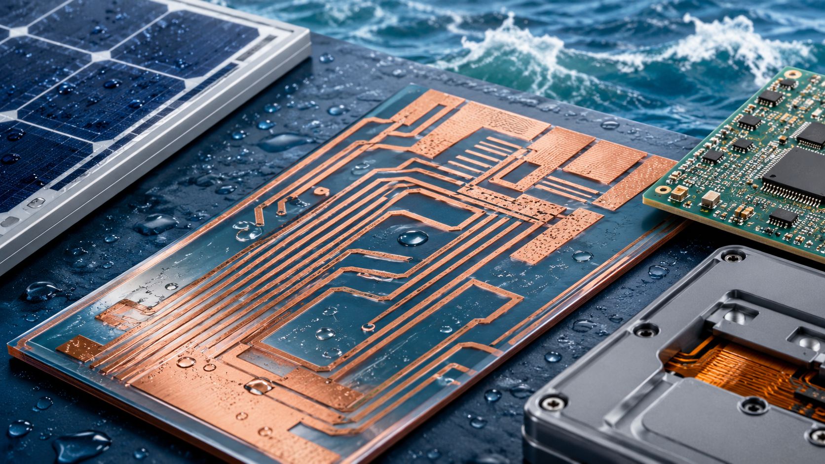
Researchers from the University of Maryland, Yale, and Lawrence Berkeley National Laboratory developed a printable copper ink that becomes conductive at 150°C, withstood six months in seawater, and can simplify the manufacture of electronic components, solar panels, and connected devices.
Researchers from the University of Maryland, Yale, and Lawrence Berkeley National Laboratory developed a printable copper ink that becomes conductive at 150°C, withstands six months in seawater, and can reduce costs, waste, and industrial steps in electronics, solar energy, and connected devices.
Copper ink advances as an option for durable electronics
A copper ink created by researchers from the University of Maryland, Yale, and Lawrence Berkeley National Laboratory withstood six months of immersion in seawater, after being printed and transformed into an electrical conductor at 150°C.
The innovation targets a long-standing problem with copper: oxidation. Although the metal is essential in electrical networks, data centers, telecommunications, electric vehicles, batteries, electronic boards, and solar panels, its exposure to air, moisture, and harsh environments requires extra protection.
-
Leaving the charger plugged in without a phone consumes energy or is it a myth? Experts call the phenomenon “phantom consumption” and warn that dozens of devices on standby can add up on the bill over the year.

-
It accompanies Earth, but it is not a moon: Chinese probe reaches Kamo’oalewa and begins an unprecedented mission to investigate where the strange asteroid came from, what its internal structure is like, and whether its origin is linked to an ancient collision that launched fragments of the lunar surface into space.
-
Space technology used to search for water on Mars is now hunting for invisible leaks under the streets of São Paulo, using satellites, AI, and chlorine signals to help Sabesp recover up to 6.7 billion liters of water.

-
Japan sends ship to extract mud rich in rare earths at nearly 6,000 meters deep in the Pacific, attempts to lift 350 tons per day from the seabed, and transforms sediments near Minamitori Island into a strategic weapon to reduce dependence on China.


These steps increase costs, consume materials, and generate waste. The formulation simplifies this path, allowing the direct printing of conductive structures on various surfaces without complex processes.
How copper ink becomes conductive
The technology starts with a blue liquid ink, developed to be deposited by printing on various materials. After heating around 150°C, it converts into conductive copper.
The low temperature expands possibilities for use on heat-sensitive materials. It can also reduce energy consumption in manufacturing compared to industrial routes that require more intense conditions.
Another relevant point is the operation in normal environmental conditions. Many copper inks require controlled atmospheres or special treatments to prevent oxidation during production. The new copper ink reduces these barriers.
Resistance in seawater expands industrial interest
The most expressive test involved the permanence of the printed structures in seawater for six months. Even when exposed to a highly corrosive environment, they did not show significant degradation.
For copper-based materials, this performance draws attention because corrosion is among the factors that increase the cost of maintenance, replacement of parts, and manufacturing of new components. In coastal or marine environments, resistance can have strategic use.
Greater durability also has an environmental effect. Fewer replacements mean less demand for mineral extraction, transportation, industrial energy, and waste disposal. This point connects the discovery to the pursuit of sustainable electronics.
Applications include solar panels and electronic boards
The researchers demonstrated the technology in conductive patterns aimed at solar cells and printed circuit boards. Both areas are important because they rely on efficient conductors and can benefit from cleaner manufacturing.
The copper ink also fits into the advancement of additive manufacturing. By depositing only the necessary material, direct printing can reduce waste compared to processes that remove parts from a larger surface.
This principle is of interest to sectors such as flexible electronics, environmental sensors, the Internet of Things, portable medical devices, and energy storage systems. In these cases, printing conductive elements on complex surfaces can speed up production.
Alternative to silver and next industrial step
The possibility of replacing silver in some applications is another point of attention. Silver has high conductivity, but its price limits large-scale use. Copper protected against oxidation can pave the way for cheaper solutions.
This cost reduction is of interest to solar panels, smart sensors, printed electronics, and connected devices. In clean technologies, reducing the initial investment can facilitate adoption in budget-restricted markets.
The transfer to the market has already begun with the creation of the company NewCopper. The challenge now is to scale up production, maintain process stability at high volume, and prove economic and environmental advantages on an industrial scale.
If these stages are overcome, copper ink could gain ground in solar energy, electric mobility, flexible electronics, and digital infrastructure. The combination of low cost, conductivity, corrosion resistance, and simplified manufacturing places the innovation among the bets for sustainable electronics.
This article was prepared based on information released by mse. The content was supported by AI tools in editorial organization and underwent human review before publication.


Be the first to react!