Portuguese
  Spanish
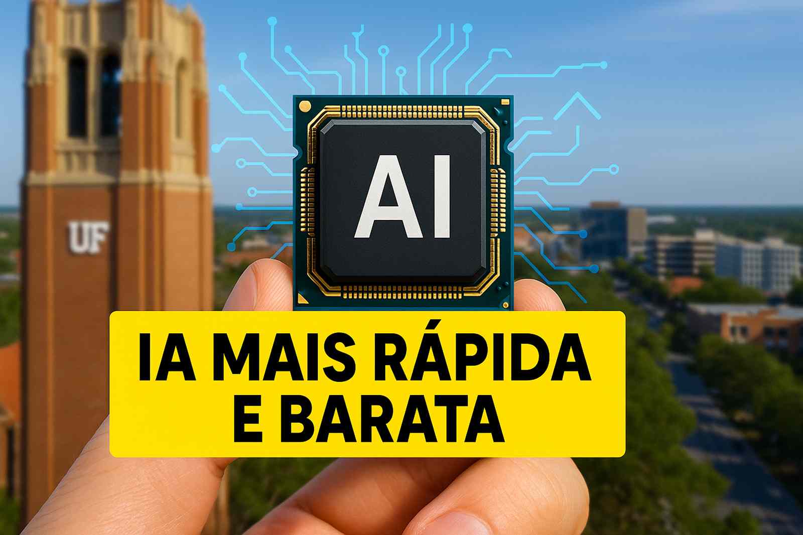
New Photonic Chip Developed at the University of Florida Combines Light and Electricity, Processes AI Tasks with Up to 100 Times More Energy Efficiency
Artificial intelligence systems are already present in almost everything, from facial recognition to automatic translations. A new chip could stand out even more in this competitive AI landscape.
However, as these models become increasingly complex, electricity consumption is rapidly growing. This demand puts pressure on electrical grids and raises concerns about sustainability.
Therefore, finding alternatives to reduce energy consumption has become a priority in technological research. It was in this context that an advancement from the University of Florida emerged.
-
World’s First Lithium-Sulfur Battery Factory Launches, Promising to Double Range Without Relying on China

-
AI Data Centers Now Feature Built-In Nuclear Power Plants and Have Ordered Non-Existent Reactors
-
In India, thousands earn about $2.50 an hour cooking and cleaning with a phone strapped to their heads, as every move is recorded to train humanoid robots for jobs they might one day replace.

-
Nuclear Fusion Study Proposes Transforming Mercury into Gold Using Tokamak Neutrons, but Real-World Application Remains Uncertain


A Chip That Combines Light and Electricity
Researchers at the institution created a new type of chip that combines light and electricity to perform fundamental AI operations.
The difference lies in the use of light to perform one of the most energy-consuming tasks: pattern recognition in images, videos, and text.
According to tests, this approach can be 10 to 100 times more efficient than traditional chips. Additionally, it accelerates processing without compromising accuracy.
Convolution with Reduced Energy
The chip was designed to perform convolution operations, essential in machine learning. These functions are responsible for identifying shapes, edges, and patterns that feed neural networks.
By integrating optical components directly onto silicon, scientists managed to conduct these operations with lasers and microscopic lenses. This drastically reduced energy consumption while maintaining performance.
“Achieving crucial machine learning computation with nearly zero energy is a leap for future AI systems,” explained Volker J. Sorger, Professor of Semiconductor Photonics at the University of Florida and lead of the study.
Practical Results of the Tests
In experiments, the prototype classified handwritten digits with about 98% accuracy. This rate is comparable to that of conventional chips but with significantly higher energy savings.
The system uses two miniature Fresnel lenses. They are flat and ultra-thin versions of those used in headlights, etched directly onto the chip. Each one is thinner than a human hair.
The process works like this: data is converted into laser light within the chip. Then, the light passes through the Fresnel lenses, which perform the necessary mathematical transformation. Afterward, the result is reconverted into a digital signal.
Color Light Multiplexing
Another advancement demonstrated that the chip can process simultaneous data streams. This is possible because different lasers, in different colors, pass through the lenses at the same time.
“We can have several wavelengths, or colors, of light passing through the lens simultaneously,” highlighted Hangbo Yang, Associate Research Professor and co-author of the work. “This is a key advantage of photonics.”
This technique is called wavelength multiplexing. In practice, it allows for more speed and efficiency compared to conventional electronic chips.
Collaboration and Future Application
The study was published in the journal Advanced Photonics and involved collaboration with UCLA, George Washington University, and the Florida Semiconductor Institute.
Sorger recalled that manufacturers like NVIDIA already use optical elements in parts of their chips. Therefore, integrating this new technology wouldn’t be far from reality.
“In the near future, chip-based optics will become an essential part of all the AI chips we use daily,” he stated. “And optical AI computing will be next.”
A Possible Turning Point for AI
The development of chips that combine light and electricity shows a path to reduce the energy burden of artificial intelligence. As the demand for computational power continues to grow, more efficient technologies are seen as a necessary solution.
Thus, the prototype from the University of Florida may pave the way for more advanced and sustainable AI models, offering speed, accuracy, and reduced consumption on a single platform.