


 Portuguese
  Spanish


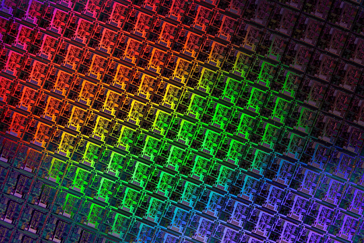

Blocked by the United States from purchasing the EUV lithography machines that manufacture the most advanced chips on the planet, Huawei presented on May 25 at ISCAS 2026, in Shanghai, the Tau Law, a framework that promises to continue densifying transistors without relying on technology that China cannot import, with a gain of more than 53% in the next Kirin chip.
He Tingbo, a board member and president of Huawei’s semiconductor arm, took the stage.
The title of the lecture was straightforward: new paths for semiconductors in practice.
The proposal tackles the root of the problem that has haunted the industry for a decade.
-
Kazakhstan’s Torysh Valley Holds Thousands of Giant Stone Spheres, Intriguing Scientists with Ancient Oceanic “Cannonballs”

-
Egypt Discovers 18 Ancient Tombs with Gold Tongues, Unveiling Unusual Funeral Rituals and Amulets Believed to Give Voice to the Dead

-
Nigeria Dumps 120 Million Tons of Sand into Atlantic to Build Massive City with 8.4 km Sea Wall for Protection Against Ocean Waves and Erosion
-
German Engineer Developed Diesel Engine Running on Vegetable Oil Decades Before Electric Cars Became Popular; Can This Forgotten Idea Work in 2026?





Moore’s Law, which has governed the sector since 1965, predicts that the number of transistors on a chip doubles every two years.
However, this geometric miniaturization has been hitting physical limits and increasingly higher costs.
As transistors reach the scale of a few nanometers, the gain per generation shrinks and the price skyrockets.
Huawei’s bet is to change the axis of the race.
Instead of continuing to shrink the transistor in space, Tau Law proposes compressing time.
The name comes from the Greek letter tau, which in engineering represents precisely the time constant of a circuit.
In other words, the goal becomes to reduce the signal propagation delay within the chip, not the physical size of each component.
How Tau Law works in practice
The central technique is called logic folding.
Instead of spreading circuits side by side, the method stacks and reorganizes the logic so that the signal travels shorter distances.
Added to this is 3D stacking, which assembles layers of circuitry on top of each other.
The result is more performance in mature manufacturing processes, without needing cutting-edge lithography.
This detail is the heart of the geopolitical play.
Extreme ultraviolet lithography, or EUV, is dominated by a single company in the world, the Dutch ASML.
Each of these machines costs about 350 million dollars and weighs the equivalent of two cargo planes.
Since 2019, the United States has pressured ASML not to sell the equipment to China.
Without EUV, therefore, Chinese manufacturers have been stuck in processes considered outdated by the industry’s forefront.
Tau Law is, in essence, the engineering response to this commercial siege.
Instead of fighting for the machine it cannot have, Huawei decided to change the very rules of the game.

According to the official statement from Huawei, this is not a laboratory promise.
The company claims to have already mass-produced 381 chips using the principles of Tau Law over the past six years.
The next Kirin chip, scheduled for fall in the northern hemisphere, will be the first to adopt the complete LogicFolding architecture.
The released numbers are impressive.
The density gain reaches 53.5%, achieving 238 million transistors per square millimeter.
The energy efficiency of high-performance cores rises by 40%.
The maximum clock increases by 12.7% and reaches 3.1 GHz.
In practice, it is the kind of leap that would normally require precisely the lithography that China cannot buy.

Why Tau Law shakes the chip war
The move fits into a broader Chinese strategy of technological self-sufficiency.
It is not the first time a company from the country has surprised without access to top lithography.
Xiaomi, for example, broke the 4 GHz barrier in a smartphone chip without using traditional big cores.
The pattern repeats: circumvent the imported limitation with creative architecture.
He Tingbo made a point of framing the announcement as an invitation, not a provocation.
According to the executive, no single company will find all the answers on the path of semiconductor evolution.
The rhetoric of openness, however, does not hide the practical effect.
If Tau Law delivers what it promises, part of the advantage that the United States tried to preserve with the EUV sanction loses strength.
Industry analysts are already discussing whether the formula is desperation, genuine advancement, or both at the same time.
The market reacted quickly: the announcement pushed semiconductor stocks up on the same day.
And Brazil in this equation
Brazil observes this board from afar.
The country does not manufacture advanced chips, does not have cutting-edge lithography, and is totally dependent on imports for any modern electronics.
The only semiconductor factory with industrial ambition, the former Ceitec, was closed in 2020.
There is now a federal plan to revive the sector, but it is still on paper, with no advanced production line in sight.
Meanwhile, the dispute between China and the United States defines who will control the technology that powers everything from cell phones to autonomous cars.
On the other hand, episodes like Tau Law show that technological monopoly is never permanent.
I confess I wonder about the long-term cost of this Brazilian absence at the table.
Each new round of the chip war makes a commodity that the country consumes by the billions more expensive and politicized, but does not produce.
Tau Law may not fulfill everything it announces, but the strategic message is already given.
When the easy path is blocked, those with engineering invent a new path.
And you, do you think Brazil still has a chance to enter the chip race or has it already fallen definitively behind? Tell us.