
 Portuguese
  Spanish
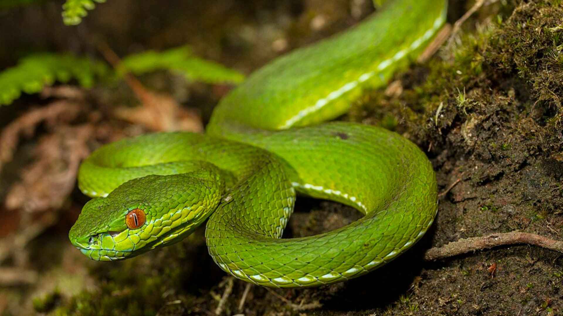
Snake-inspired technology combines CMOS sensors and infrared conversion to enhance high-definition artificial vision, with applications pointed out by the authors in night vision, autonomous driving, industrial inspection, and medical diagnosis, without relying on the bulky systems used in advanced thermal imaging.
Researchers from the Beijing Institute of Technology in China have developed an artificial vision system capable of capturing 4K images in short and medium-wave infrared, a spectrum range not captured by conventional silicon cameras.
Described in the journal Light: Science & Applications, the technology combines CMOS sensors with a converter that transforms infrared radiation into visible light, allowing the information to be processed by a base already used in most digital cameras.
According to the authors, the proposal seeks to overcome limitations of high-performance infrared imaging, which often relies on specific materials, more complex architectures, and, in many cases, cooling systems to reduce noise in the captured signal.
-
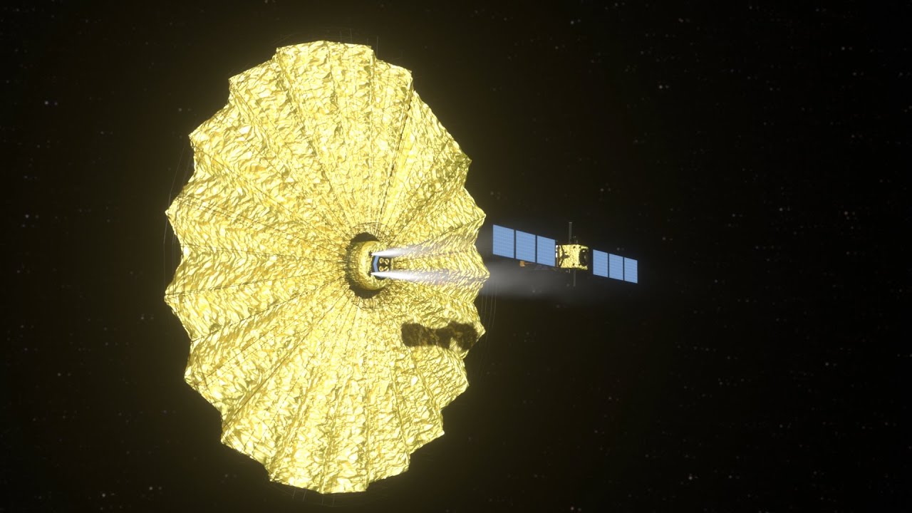
NASA’s Giant “Space Flower” to Unveil Earth-like Planets by Blocking Distant Stars’ Light

-
A 13-foot robot nicknamed Godzilla is assembling the world’s largest nuclear fusion reactor piece by piece.
-
Three-Year-Old Fulfills Dream of Joining Garbage Collectors in Brazil, Captivates Thousands Online with Heartwarming Video

-
Experts Warn: Aging NASA Launch Facilities Could Hinder Artemis Moon Mission Progress


Instead of following this model, the team integrated the converter directly into CMOS sensors, a platform consolidated in the electronic imaging industry and present in devices such as digital cameras, smartphones, surveillance systems, and computer vision equipment.
The system achieved a resolution of 3840 by 2160 pixels, a standard associated with 4K, with a pixel pitch of 1.55 micrometers, a measure used to indicate the distance between the centers of neighboring pixels on the sensor.
According to the scientific publication, the integration allowed short and medium-wave infrared imaging at room temperature, without the use of cryogenic cooling, a resource employed in some specialized infrared detectors.
Snake-inspired camera
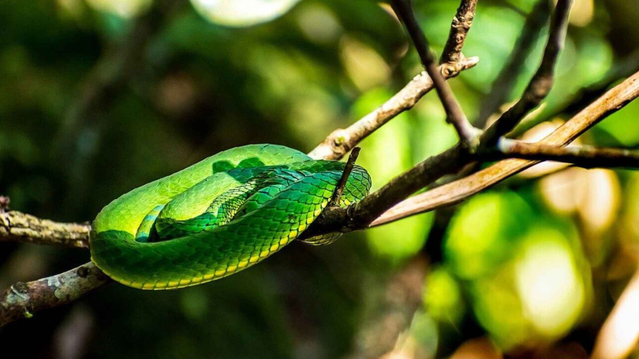
The inspiration came from the pit organs present in some snakes, structures sensitive to infrared radiation emitted by warm bodies and associated with these animals’ ability to perceive thermal signals in low-light environments.
In nature, this mechanism helps snakes identify environmental information that does not rely solely on visible light, a characteristic that served as a reference for the architecture developed by Chinese researchers.
In the system described by the team, the biological principle was adapted to an electronic solution based on optical conversion, in which infrared radiation is transformed into visible light before being read by the sensor.
The converter functions as an intermediate layer between the infrared and the silicon CMOS, allowing a conventional reading base to register information located outside the range normally captured by common cameras.
This strategy is not based on estimating invisible information through software or post-processing, but on expanding the spectral range physically detected by the device before the image reading and interpretation stage.
How the sensor sees infrared
Traditional CMOS sensors are compact, mass-produced, and widely used in the industry, but they have natural limitations when capturing involves wavelengths beyond the visible range of the electromagnetic spectrum.
Infrared radiation, especially in the short and medium wave bands, requires materials and structures capable of interacting with wavelengths that are not efficiently absorbed by conventional silicon.
To overcome this limitation, the researchers used colloidal quantum dots of mercury telluride, a material mentioned in the study for its ability to absorb infrared radiation in longer spectrum bands.
These dots were organized in a barrier heterojunction, a structure developed to reduce dark current, a type of noise associated with heat that can degrade signal quality in detectors operating at room temperature.
The architecture also incorporates layers of zinc oxide and P3HT polymer, used to block unwanted charges without impeding the transport of carriers related to the useful signal described by the researchers.
According to the authors, this combination of materials and electronic barriers helped maintain the system’s sensitivity without resorting to cryogenic cooling methods, which increase the complexity of traditional infrared detectors.

In addition to detecting infrared radiation, the device performs the conversion to visible emission, a process that allows the CMOS sensor to record information that, under normal conditions, would be outside its response range.
With this approach, data captured in a region invisible to the human eye can be converted into signals compatible with a silicon base used in commercial electronic imaging platforms.
Infrared Image in 4K
The team reports that the converters were integrated into CMOS sensors on a wafer scale, including an 8-inch silicon wafer, a format associated with industrial processes for manufacturing electronic components.
This data was highlighted by the researchers because it points to compatibility with production stages already used in the semiconductor industry, although the study does not present the technology as a commercially available product.
In the demonstrations reported in the scientific publication, the system produced short and medium-wave infrared images with 4K resolution and a rate of 120 frames per second.
The same platform was used to visualize through silicon wafers and generate thermal images of heat sources, two applications used in the study to demonstrate the system’s response under different conditions.
Another data presented by the authors is the expansion of the detectable spectral range, with a response extending from the visible region to 4.5 micrometers in the medium-wave infrared.
According to the study, this range represents an expansion of about 14 times compared to the range normally accessible to conventional silicon cameras, considering the material’s limitation in detecting longer wavelengths.
This spectral coverage can be useful, as indicated by the researchers, in environments where visible light offers less information, such as scenes with smoke, fog, low lighting, or reduced contrast between objects.
Even with the described results, the technology remains in the context of scientific research, and the study does not provide timelines, final costs, or commercial plans for adoption in consumer devices.
CMOS Sensors and Thermal Imaging

Infrared imaging is already used in areas such as industrial inspection, night vision, remote sensing, and security equipment, especially when capturing visible light does not provide sufficient data about a scene.
In systems with higher sensitivity, infrared detectors often use specialized materials, specific optical components, and cooling solutions that increase the size, power consumption, and operational complexity of the equipment.
By integrating infrared conversion into CMOS sensors, the research presents a path to bring this capability closer to already established platforms in image electronics, according to the authors’ interpretation of the study.
In this model, the described technical advantage is not only in visualizing thermal sources but in the possibility of adding new bands of information to sensors manufactured on a silicon base.
The authors cite possible applications in autonomous driving, industrial inspection, smart manufacturing, medical diagnostics, food safety, gas sensing, and night vision, areas that rely on information not always visible in traditional cameras.
In a production line, for example, infrared capture can help identify patterns or defects that do not appear under common lighting, provided the system is adapted to the demands of the industrial environment.
In mobility, sensors with greater spectral range can complement conventional cameras in low visibility situations, although any application in autonomous driving depends on additional validations of safety, integration, and reliability.
Challenges before commercial use
Despite the reported results, the study does not eliminate the challenges involved in the large-scale adoption of infrared sensors, especially in aspects such as durability, manufacturing uniformity, production cost, and integration into final systems.
There also remain issues related to the use of materials with mercury, as applications outside the laboratory would require safe manufacturing processes, encapsulation, environmental control, and proper disposal of the components used.
The research itself informs that mercury telluride requires care during material synthesis and device preparation, a relevant point for evaluating future development stages and potential technology transfer.
In the stage described by the scientists, the combination of 4K resolution, room temperature operation, and integration with CMOS characterizes a high-performance experimental demonstration for infrared imaging.
The technology, as presented in the publication, seeks to bring infrared vision closer to less bulky formats and more compatible with electronics already produced on a scale by the sensor industry.
By adapting a capability associated with snakes to a silicon electronic architecture, the study expands the research field on cameras capable of recording information beyond visible light.
The development shows that the evolution of digital imaging can also go through the expansion of the spectral ranges captured by sensors, not just by increasing resolution or computational processing applied to images.


