Portuguese
  Spanish
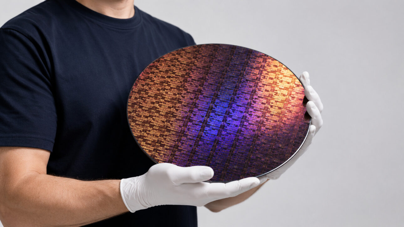
Experimental technology announced by IBM combines stacked transistors, higher performance, and energy efficiency to drive future generations of artificial intelligence and advanced computing.
A groundbreaking innovation for the semiconductor industry was presented by IBM Research on June 25, 2026.
The company unveiled an experimental 0.7-nanometer technology, also identified as a 7-angstrom process.
According to IBM, the new architecture could gather nearly 100 billion transistors in an area similar to the size of a fingernail.
-
Apple Raises MacBook and iPad Prices as Memory Costs Surge by Up to 98%, Losing Edge Over Rivals and Highlighting AI Boom’s Impact on Consumers

-
China Establishes State Centers to Train Humanoid Robots, While the West Lags Behind with Makeshift Solutions
-
The Trap of Modern Technology: How Screen Overload and Digital Connections Can Impact Your Mental Health and Well-being
-
Wyoming Couple Grows Tropical Fruits Year-Round in -40°C Using Geothermal Greenhouse, Demonstrating Earth’s Heat Can Produce Oranges and Lemons in Snow Without Traditional Heating


The technology also promises up to 50% more performance or up to 70% more energy efficiency compared to the previous generation.
The component, however, remains in the research phase. The novelty does not yet represent a commercial processor ready for cell phones, computers, or automobiles.
0.7-nanometer technology expands chip capacity
The scale reduction allows for a greater number of transistors to be installed within an extremely small space.
This advancement could increase processing capacity without requiring physically larger devices.
The evolution becomes especially relevant in light of the growth of artificial intelligence, cell phones, and advanced computing systems.
Data presented by IBM Research indicate that the technology nearly doubles the density of the experimental 2-nanometer chip, announced in May 2021.
The previous generation gathered about 50 billion transistors in an area comparable to the size of a fingernail.
The 0.7-nanometer process could raise this amount to nearly 100 billion transistors in the same space.
Three-dimensional architecture stacks the transistors
One of the main differentiators of the project is the structure called nanostack.
The transistors are no longer distributed only side by side on the surface of the chip.
The new architecture allows components to be stacked vertically in different layers, increasing the available density.
This organization makes better use of internal space and can reduce energy consumption during processing.
The evolution of semiconductors, therefore, no longer depends exclusively on the production of smaller components.
Companies and research centers are also seeking new ways to organize transistors near the physical limits of the nanometric scale.
Performance and energy efficiency gain prominence
The projections released by IBM indicate that the technology could offer up to 50% more performance.
Another configuration could prioritize up to 70% more energy efficiency, maintaining a capacity similar to the previous generation.
The manufacturer can choose between increasing processing power or reducing electricity consumption, depending on the application.
Among the possible uses of the technology are:
- advanced artificial intelligence systems;
- cell phones with greater processing capacity;
- smart and connected vehicles;
- more efficient data centers;
- advanced computing infrastructure.
The disclosed benefits still need to be confirmed during industrial development and large-scale manufacturing.
Technology may take years to reach the market
The relevance of the announcement does not mean that the chip will be launched immediately.
IBM estimates that possible commercial production could begin in approximately five years.
The company has not yet revealed which manufacturer might produce the future components.
The presented results represent technical projections, not the performance of a product currently available on the market.
Challenges related to costs, materials, and large-scale production will still need to be overcome.
A breakthrough that goes beyond miniaturization
IBM’s announcement reinforces an important transformation in the global semiconductor industry.
The evolution of chips previously depended mainly on reducing the size of transistors.
New three-dimensional architectures and stacking techniques now help to maintain the advancement of computing.
“We are not just creating smaller transistors. We are reinventing how chips are built,” said Jay Gambetta, director of IBM Research, at the announcement.
The nanostack architecture could support future generations of artificial intelligence, electronic devices, and high-performance computing.
The information was released by IBM Research on June 25, 2026 and echoed by the international agency Reuters.
Which application of this technology could have the greatest impact: faster cell phones, more advanced artificial intelligence, or more economical computers? Leave your opinion in the comments.