 Portuguese
  English
  Spanish
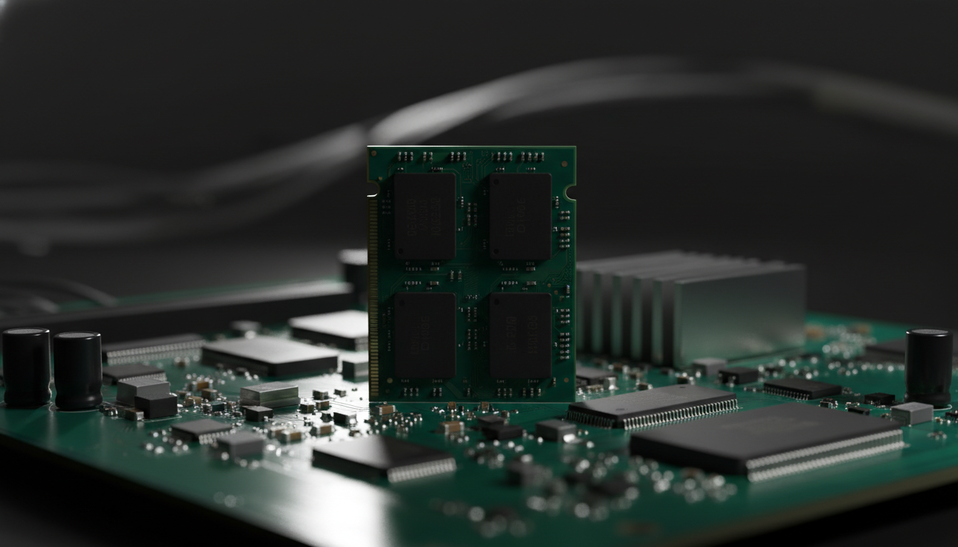
While conventional electronic memories fail in low orbit after about 30,000 rads of accumulated radiation, researchers at Georgia Tech have presented a ferroelectric NAND flash memory that remains stable up to 1 million rads, according to a study published on May 18, 2026, by the Interesting Engineering group.
The value is equivalent to 100 million consecutive medical X-rays on the same chip. The barrier places, for the first time, a practical storage memory within the window needed for NASA missions beyond Jupiter, such as Europa Clipper and subsequent proposals.
The leader of the work is Asif Khan, an associate professor at the School of Electrical and Computer Engineering at Georgia Tech, with doctoral student Lance Fernandes as the first author.
-
Three Chinese companies manufacture more than 96% of the world’s dry cargo containers and 100% of refrigerated ones, in a dominance built over 40 years that has made it almost impossible for the West to compete in this market.

-
Argentina confirms Belgian giant to lead strategic Paraná River waterway and promises to reduce logistical costs on one of South America’s most important routes

-
MBRF surprises the logistics sector by demonstrating how Artificial Intelligence can directly influence deliveries throughout Brazil by reorganizing distribution routes in seconds, optimizing fleet usage, reducing logistics costs, and speeding up product arrivals even in the face of unforeseen road incidents.
-
With deep ports and strategic railway, Espírito Santo advances to compete with Santos and attract foreign trade cargo.


The article was published in the scientific journal Nano Letters of the American Chemical Society.
What ferroelectric memory does differently from common NAND
Conventional NAND memory stores data as electrical charges trapped in transistors. A charged particle from space can remove this charge, altering the recorded bit.
Above 100,000 rads, bit error becomes frequent.
As detailed in the paper by Asif Khan and Lance Fernandes in Nano Letters, Georgia Tech’s ferroelectric NAND memory does not use trapped charges.
Data is stored as polarization in hafnium oxide material.
Polarization operates at the atomic level, with electrons fixed in the material’s structural position. Therefore, it resists direct radiation without losing information, even under bombardment of ionizing particles.
In parallel, hafnium oxide combines 2 advantages. It has been integrated into commercial chip manufacturing processes since 2007. And it can be stacked in three-dimensional structures like modern 3D NAND.
The numbers separating low orbit from a mission to Jupiter
The radiation environment varies dramatically depending on the orbit. According to NASA engineering data, satellites in low Earth orbit accumulate between 5,000 and 30,000 rads over their lifespan, usually 5 to 15 years.
According to the NASA JPL, geostationary satellites 36,000 km from Earth receive from 100,000 to 300,000 rads.
The Europa Clipper, launched in October 2024 towards Jupiter’s moon Europa, will need to operate above 1 million rads.
The problem is structural. Jupiter has the second strongest magnetic field in the Solar System, after the Sun. The planet’s 4 radiation belts create a lethal dose for electronics without specific shielding.
In parallel, past missions have shown the limit. The Galileo probe, in orbit around Jupiter from 1995 to 2003, progressively lost parts of its memory.
The Cassini spacecraft operated in Saturn from 2004 to 2017 with 9 scientific instruments, several affected by radiation.

Technical reveal: how hafnium oxide stores data under bombardment
In the background, Georgia Tech’s memory operates on 3 technical principles different from conventional NAND.
The first is the use of ultrathin films of hafnium oxide. The typical thickness is 10 nanometers. This layer exhibits spontaneous ferroelectric property, discovered in 2011 by German researchers at NaMLab.
The second is storage by polarization. Unlike conventional NAND flash, the ferroelectric cell defines the bit by the orientation of the material’s electric dipole, not by the amount of charges trapped in a floating layer.
The third is tolerance to direct radiation. According to the paper by Khan and Fernandes, controlled exposures up to 1 million rads in gamma rays maintained the correct reading of the tested chips.
The result surpasses by 10 times the best commercial standard currently certified for space missions.
Above all, the technology is compatible with 2 industrial pillars. Chip manufacturing processes have used hafnium oxide in transistors since 2007, after Intel’s transition to the 45-nanometer node.
And the 3D NAND architecture, dominant today in SSDs, can be adapted for the ferroelectric version.
How the space sector worked before
The space electronics industry has so far used a combination of 3 strategies. The first was physically shielding the equipment with aluminum vaults.
The Europa Clipper carries a 6.5-millimeter-thick vault around critical electronics.
According to EE Times, the second strategy is to use common SLC NAND memory from Micron Technology pre-qualified for radiation.
The Micron M73A delivers 256 Gbit per chip and tolerates tens of thousands of rads.
The third strategy is redundancy. Each critical calculation is performed in parallel on 3 or 4 processors, and the result is decided by voting.
This scheme, called “triple modular redundancy,” consumes triple the electrical consumption and weight.
On the other hand, all 3 strategies have limits. Shielding increases weight and launch cost by thousands of dollars per kilogram.
Redundancy doubles the budget. Pre-qualification does not cover the regime above 300,000 rads.

Human reveal: Lance Fernandes and the research that became the cover of Nano Letters
The human face of the discovery is Lance Fernandes, a doctoral student in Electrical and Computer Engineering at Georgia Tech. He is the first author of the paper published in Nano Letters in May 2026.
As cited by Interesting Engineering, Fernandes coordinated gamma ray tests at the University’s accelerator. The full paper is available in open format on the American Chemical Society server under DOI 10.1021/acs.nanolett.5c05947.
The group leader is Asif Khan, an associate professor with 12 years of career at Georgia Tech. His main area is ferroelectric materials for low-power electronics.
The laboratory has about 8 active researchers in 2026.
In parallel, the work connects 3 institutions. Besides Georgia Tech, it had technical collaboration from NaMLab in Germany, a pioneer in the ferroelectric use of hafnium oxide, and NASA’s Goddard Space Flight Center, a specialist in space electronics qualification.
Comparison with Micron, Honeywell, and 3D Plus
The rad-hardened memory market currently has 4 main suppliers. Micron Technology produces the pre-qualified M73A SLC NAND, with 256 Gbit per chip and tolerance of a few hundred thousand rads.
Honeywell offers SOI memories and rad-hard FPGAs for military satellites. BAE Systems operates in the defense segment. 3D Plus, a French company, makes integrated modules for the European Space Agency.
According to EE Times, the global space memory segment moves about $1.2 billion in 2025. Georgia Tech’s ferroelectric NAND could redefine this market if the path to flight qualification is completed in the next 5 years.
In parallel, the Europa Clipper is already flying en route to Jupiter since October 2024. It arrives in April 2030 and uses the technology available in 2020.
The next mission to Jupiter, still in project by NASA, could be a natural candidate for ferroelectric memory.

Future reveal: the path to the first NASA flight in 2030
The next step for Khan and Fernandes’ team is industrial qualification for space flight. The standard process requires 4 successive phases.
Laboratory characterization, integration with controller, tests in simulated environments, and demonstration in low orbit.
Each typical phase takes between 18 and 24 months. Considering the paper published in May 2026, a reasonable estimate is that the technology will be ready for flight in a NASA mission from 2031 or 2032.
According to IEEE Spectrum analysis, typical NASA missions have a design cycle of 8 to 12 years from conception to launch. The window is compatible with Europa Lander or Uranus Orbiter, both under study by NASA for the 2030s.
It is worth remembering the coverage of centralized digital platforms as a reference for other comparable technological leaps.
- Radiation tolerance: 1,000,000 rads (1 million)
- Equivalence: 100 million medical X-rays
- Material: 10 nm hafnium oxide film
- Mechanism: ferroelectric polarization (not trapped charges)
- Leader: Asif Khan, Georgia Tech (12-year career)
- 1st author: Lance Fernandes (doctoral student)
- Publication: Nano Letters, DOI 10.1021/acs.nanolett.5c05947
- NASA flight window: 2031-2032 (reasonable estimate)

The points that still depend on industrial validation
Despite the scientific leap, 3 fronts still depend on industrial validation. The first is large-scale manufacturing in commercial foundries like TSMC, Samsung, or Micron.
On the other hand, integration with conventional SATA and PCIe controllers requires firmware adaptation. The third front is the qualification cycle for orbital flight, with space environment simulations in a dedicated chamber for consecutive months.


Be the first to react!